|
|
|
PDF AD9752 Data sheet ( Hoja de datos )
| Número de pieza | AD9752 | |
| Descripción | 12-Bit/ 125 MSPS High Performance TxDAC D/A Converter | |
| Fabricantes | Analog Devices | |
| Logotipo | ||
Hay una vista previa y un enlace de descarga de AD9752 (archivo pdf) en la parte inferior de esta página. Total 23 Páginas | ||
|
No Preview Available !
a
12-Bit, 125 MSPS High Performance
TxDAC® D/A Converter
AD9752*
FEATURES
High Performance Member of Pin-Compatible
TxDAC Product Family
125 MSPS Update Rate
12-Bit Resolution
Excellent Spurious Free Dynamic Range Performance
SFDR to Nyquist @ 5 MHz Output: 79 dBc
Differential Current Outputs: 2 mA to 20 mA
Power Dissipation: 185 mW @ 5 V
Power-Down Mode: 20 mW @ 5 V
On-Chip 1.20 V Reference
CMOS-Compatible +2.7 V to +5.5 V Digital Interface
Package: 28-Lead SOIC and TSSOP
Edge-Triggered Latches
APPLICATIONS
Wideband Communication Transmit Channel:
Direct IF
Basestations
Wireless Local Loop
Digital Radio Link
Direct Digital Synthesis (DDS)
Instrumentation
PRODUCT DESCRIPTION
The AD9752 is a 12-bit resolution, wideband, second generation
member of the TxDAC series of high performance, low power
CMOS digital-to-analog-converters (DACs). The TxDAC family,
which consists of pin compatible 8-, 10-, 12-, and 14-bit DACs, is
specifically optimized for the transmit signal path of communica-
tion systems. All of the devices share the same interface options,
small outline package and pinout, thus providing an upward or
downward component selection path based on performance,
resolution and cost. The AD9752 offers exceptional ac and dc
performance while supporting update rates up to 125 MSPS.
The AD9752’s flexible single-supply operating range of 4.5 V to
5.5 V and low power dissipation are well suited for portable and
low power applications. Its power dissipation can be further
reduced to a mere 65 mW, without a significant degradation in
performance, by lowering the full-scale current output. Also, a
power-down mode reduces the standby power dissipation to
approximately 20 mW.
The AD9752 is manufactured on an advanced CMOS process.
A segmented current source architecture is combined with a
proprietary switching technique to reduce spurious components
and enhance dynamic performance. Edge-triggered input latches
and a 1.2 V temperature compensated bandgap reference have
been integrated to provide a complete monolithic DAC solution.
The digital inputs support +2.7 V to +5 V CMOS logic families.
TxDAC is a registered trademark of Analog Devices, Inc.
*Protected by U.S. Patents Numbers 5450084, 5568145, 5689257, 5612697 and
5703519. Other patents pending.
REV. 0
Information furnished by Analog Devices is believed to be accurate and
reliable. However, no responsibility is assumed by Analog Devices for its
use, nor for any infringements of patents or other rights of third parties
which may result from its use. No license is granted by implication or
otherwise under any patent or patent rights of Analog Devices.
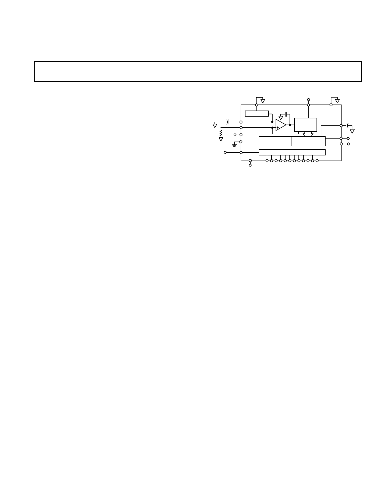
FUNCTIONAL BLOCK DIAGRAM
+5V
0.1F
RSET +5V
CLOCK
REFLO
+1.20V REF
REFIO
FS ADJ
150pF
AVDD ACOM
CURRENT
SOURCE
ARRAY
AD9752
ICOMP 0.1F
DVDD
DCOM
SEGMENTED
SWITCHES
LSB
SWITCHES
IOUTA
IOUTB
CLOCK
SLEEP
LATCHES
DIGITAL DATA INPUTS (DB11–DB0)
The AD9752 is a current-output DAC with a nominal full-scale
output current of 20 mA and > 100 kΩ output impedance.
Differential current outputs are provided to support single-
ended or differential applications. Matching between the two
current outputs ensures enhanced dynamic performance in a
differential output configuration. The current outputs may be
tied directly to an output resistor to provide two complemen-
tary, single-ended voltage outputs or fed directly into a trans-
former. The output voltage compliance range is 1.25 V.
The on-chip reference and control amplifier are configured for
maximum accuracy and flexibility. The AD9752 can be driven
by the on-chip reference or by a variety of external reference
voltages. The internal control amplifier, which provides a wide
(>10:1) adjustment span, allows the AD9752 full-scale current
to be adjusted over a 2 mA to 20 mA range while maintaining
excellent dynamic performance. Thus, the AD9752 may oper-
ate at reduced power levels or be adjusted over a 20 dB range to
provide additional gain ranging capabilities.
The AD9752 is available in 28-lead SOIC and TSSOP packages.
It is specified for operation over the industrial temperature range.
PRODUCT HIGHLIGHTS
1. The AD9752 is a member of the wideband TxDAC product
family that provides an upward or downward component selec-
tion path based on resolution (8 to 14 bits), performance and
cost. The entire family of TxDACs is available in industry
standard pinouts.
2. Manufactured on a CMOS process, the AD9752 uses a
proprietary switching technique that enhances dynamic
performance beyond that previously attainable by higher
power/cost bipolar or BiCMOS devices.
3. On-chip, edge-triggered input CMOS latches interface readily
to +2.7 V to +5 V CMOS logic families. The AD9752 can
support update rates up to 125 MSPS.
4. A flexible single-supply operating range of 4.5 V to 5.5 V and
a wide full-scale current adjustment span of 2 mA to 20 mA
allow the AD9752 to operate at reduced power levels.
5. The current output(s) of the AD9752 can be easily config-
ured for various single-ended or differential circuit topologies.
One Technology Way, P.O. Box 9106, Norwood, MA 02062-9106, U.S.A.
Tel: 781/329-4700 World Wide Web Site: http://www.analog.com
Fax: 781/326-8703
© Analog Devices, Inc., 1999
1 page 
PIN CONFIGURATION
(MSB) DB11 1
28 CLOCK
DB10 2
27 DVDD
DB9 3
26 DCOM
DB8 4
25 NC
DB7 5 AD9752 24 AVDD
DB6 6 TOP VIEW 23 ICOMP
DB5 7 (Not to Scale) 22 IOUTA
DB4 8
21 IOUTB
DB3 9
20 ACOM
DB2 10
19 NC
DB1 11
18 FS ADJ
DB0 12
17 REFIO
NC 13
16 REFLO
NC 14
15 SLEEP
NC = NO CONNECT
AD9752
PIN FUNCTION DESCRIPTIONS
Pin No.
1
2–11
12
13, 14,
19, 25
15
16
17
18
19
20
21
22
23
24
26
27
28
Name
Description
DB11
Most Significant Data Bit (MSB).
DB10–DB1 Data Bits 1–10.
DB0 Least Significant Data Bit (LSB).
NC
SLEEP
REFLO
REFIO
FS ADJ
NC
ACOM
IOUTB
IOUTA
ICOMP
AVDD
DCOM
DVDD
CLOCK
No Internal Connection.
Power-Down Control Input. Active High. Contains active pull-down circuit, thus may be left unterminated
if not used.
Reference Ground when Internal 1.2 V Reference Used. Connect to AVDD to disable internal reference.
Reference Input/Output. Serves as reference input when internal reference disabled (i.e., Tie REFLO to
AVDD). Serves as 1.2 V reference output when internal reference activated (i.e., Tie REFLO to ACOM).
Requires 0.1 µF capacitor to ACOM when internal reference activated.
Full-Scale Current Output Adjust.
No Connect.
Analog Common.
Complementary DAC Current Output. Full-scale current when all data bits are 0s.
DAC Current Output. Full-scale current when all data bits are 1s.
Internal Bias Node for Switch Driver Circuitry. Decouple to ACOM with 0.1 µF capacitor.
Analog Supply Voltage (+4.5 V to +5.5 V).
Digital Common.
Digital Supply Voltage (+2.7 V to +5.5 V).
Clock Input. Data latched on positive edge of clock.
REV. 0
–5–
5 Page 
AD9752
The second method may be used in a dual-supply system in
which the common-mode voltage of REFIO is fixed and IREF is
varied by an external voltage, VGC, applied to RSET via an ampli-
fier. An example of this method is shown in Figure 21, in which
the internal reference is used to set the common-mode voltage
of the control amplifier to 1.20 V. The external voltage, VGC, is
referenced to ACOM and should not exceed 1.2 V. The value
of RSET is such that IREFMAX and IREFMIN do not exceed 62.5 µA
and 625 µA, respectively. The associated equations in Figure 21
can be used to determine the value of RSET.
AVDD
REFLO 150pF
+1.2V REF
AVDD
REFIO
1F FS ADJ
RSET IREF AD9752
CURRENT
SOURCE
ARRAY
VGC
IREF = (1.2–VGC)/RSET
WITH VGC < VREFIO AND 62.5A Յ IREF Յ 625A
Figure 21. Dual-Supply Gain Control Circuit
ANALOG OUTPUTS
The AD9752 produces two complementary current outputs,
IOUTA and IOUTB, which may be configured for single-end
or differential operation. IOUTA and IOUTB can be converted
into complementary single-ended voltage outputs, VOUTA and
VOUTB, via a load resistor, RLOAD, as described in the DAC
Transfer Function section by Equations 5 through 8. The
differential voltage, VDIFF, existing between VOUTA and VOUTB
can also be converted to a single-ended voltage via a transformer
or differential amplifier configuration.
Figure 22 shows the equivalent analog output circuit of the
AD9752 consisting of a parallel combination of PMOS differen-
tial current switches associated with each segmented current
source. The output impedance of IOUTA and IOUTB is deter-
mined by the equivalent parallel combination of the PMOS
switches and is typically 100 kΩ in parallel with 5 pF. Due to
the nature of a PMOS device, the output impedance is also
slightly dependent on the output voltage (i.e., VOUTA and VOUTB)
and, to a lesser extent, the analog supply voltage, AVDD, and
full-scale current, IOUTFS. Although the output impedance’s
signal dependency can be a source of dc nonlinearity and ac linear-
ity (i.e., distortion), its effects can be limited if certain precau-
tions are noted.
AVDD
IOUTA
RLOAD
IOUTB
RLOAD
Figure 22. Equivalent Analog Output
IOUTA and IOUTB also have a negative and positive voltage
compliance range. The negative output compliance range of
–1.0 V is set by the breakdown limits of the CMOS process.
Operation beyond this maximum limit may result in a break-
down of the output stage and affect the reliability of the AD9752.
The positive output compliance range is slightly dependent on
the full-scale output current, IOUTFS. It degrades slightly from its
nominal 1.25 V for an IOUTFS = 20 mA to 1.00 V for an IOUTFS =
2 mA. Operation beyond the positive compliance range will
induce clipping of the output signal which severely degrades
the AD9752’s linearity and distortion performance.
For applications requiring the optimum dc linearity, IOUTA
and/or IOUTB should be maintained at a virtual ground via an
I-V op amp configuration. Maintaining IOUTA and/or IOUTB
at a virtual ground keeps the output impedance of the AD9752
fixed, significantly reducing its effect on linearity. However,
it does not necessarily lead to the optimum distortion perfor-
mance due to limitations of the I-V op amp. Note that the
INL/DNL specifications for the AD9752 are measured in
this manner using IOUTA. In addition, these dc linearity
specifications remain virtually unaffected over the specified
power supply range of 4.5 V to 5.5 V.
Operating the AD9752 with reduced voltage output swings at
IOUTA and IOUTB in a differential or single-ended output
configuration reduces the signal dependency of its output
impedance thus enhancing distortion performance. Although
the voltage compliance range of IOUTA and IOUTB extends
from –1.0 V to +1.25 V, optimum distortion performance is
achieved when the maximum full-scale signal at IOUTA and
IOUTB does not exceed approximately 0.5 V. A properly se-
lected transformer with a grounded center-tap will allow the
AD9752 to provide the required power and voltage levels to
different loads while maintaining reduced voltage swings at
IOUTA and IOUTB. DC-coupled applications requiring a
differential or single-ended output configuration should size
RLOAD accordingly. Refer to Applying the AD9752 section for
examples of various output configurations.
The most significant improvement in the AD9752’s distortion
and noise performance is realized using a differential output
configuration. The common-mode error sources of both
IOUTA and IOUTB can be substantially reduced by the
common-mode rejection of a transformer or differential am-
plifier. These common-mode error sources include even-
order distortion products and noise. The enhancement in
distortion performance becomes more significant as the recon-
structed waveform’s frequency content increases and/or its
amplitude decreases.
The distortion and noise performance of the AD9752 is also
slightly dependent on the analog and digital supply as well as the
full-scale current setting, IOUTFS. Operating the analog supply at
5.0 V ensures maximum headroom for its internal PMOS current
sources and differential switches leading to improved distortion
performance. Although IOUTFS can be set between 2 mA and
20 mA, selecting an IOUTFS of 20 mA will provide the best dis-
tortion and noise performance also shown in Figure 8. The
noise performance of the AD9752 is affected by the digital sup-
ply (DVDD), output frequency, and increases with increasing
clock rate as shown in Figure 11. Operating the AD9752 with
low voltage logic levels between 3 V and 3.3 V will slightly re-
duce the amount of on-chip digital noise.
REV. 0
–11–
11 Page | ||
| Páginas | Total 23 Páginas | |
| PDF Descargar | [ Datasheet AD9752.PDF ] | |
Hoja de datos destacado
| Número de pieza | Descripción | Fabricantes |
| AD9750 | 10-Bit/ 125 MSPS High Performance TxDAC D/A Converter | Analog Devices |
| AD9751 | 10-Bit 300 MSPS High-Speed TxDAC+ D/A Converter | Analog Devices |
| AD9752 | 12-Bit/ 125 MSPS High Performance TxDAC D/A Converter | Analog Devices |
| AD9753 | 12-Bit 300 MSPS High-Speed TxDAC+ D/A Converter | Analog Devices |
| Número de pieza | Descripción | Fabricantes |
| SLA6805M | High Voltage 3 phase Motor Driver IC. |
Sanken |
| SDC1742 | 12- and 14-Bit Hybrid Synchro / Resolver-to-Digital Converters. |
Analog Devices |
|
DataSheet.es es una pagina web que funciona como un repositorio de manuales o hoja de datos de muchos de los productos más populares, |
| DataSheet.es | 2020 | Privacy Policy | Contacto | Buscar |