|
|
PDF AD9712B Data sheet ( Hoja de datos )
| Número de pieza | AD9712B | |
| Descripción | 12-Bit/ 100 MSPS D/A Converters | |
| Fabricantes | Analog Devices | |
| Logotipo |  |
|
Hay una vista previa y un enlace de descarga de AD9712B (archivo pdf) en la parte inferior de esta página. Total 12 Páginas | ||
|
No Preview Available !
a
12-Bit, 100 MSPS
D/A Converters
FEATURES
100 MSPS Update Rate
ECL/TTL Compatibility
SFDR @ 1 MHz: 70 dBc
Low Glitch Impulse: 28 pV-s
Fast Settling: 27 ns
Low Power: 725 mW
1/2 LSB DNL (B Grade)
40 MHz Multiplying Bandwidth
APPLICATIONS
ATE
Signal Reconstruction
Arbitrary Waveform Generators
Digital Synthesizers
Signal Generators
GENERAL DESCRIPTION
The AD9712B and AD9713B D/A converters are replacements
for the AD9712 and AD9713 units which offer improved ac and
dc performance. Like their predecessors, they are 12-bit, high
speed digital-to-analog converters fabricated in an advanced
oxide isolated bipolar process. The AD9712B is an ECL-
compatible device featuring update rates of 100 MSPS mini-
mum; the TTL-compatible AD9713B will update at 80 MSPS
minimum.
AD9712B/AD9713B
FUNCTIONAL BLOCK DIAGRAM
LATCH 26
ENABLE
28
DIGITAL
INPUTS
D1
THRU
D12
1
AD9712B/AD9713B
(MSB)
DECODERS
AND
DRIVERS
SWITCH
NETWORK
11 (LSB)
R SET 24
INTERNAL
VOLTAGE
REFERENCE
+
CONTROL
AMP
–
20
REFERENCE
OUT
19
CONTROL
AMP IN
14 I OUT
16 I OUT
17 REFERENCE
IN
18 CONTROL
AMP OUT
Designed for direct digital synthesis, waveform reconstruction,
and high resolution imaging applications, both devices feature
low glitch impulse of 28 pV-s and fast settling times of 27 ns.
Both units are characterized for dynamic performance and have
excellent harmonic suppression.
The AD9712B and AD9713B are available in 28-pin plastic
DIPs and PLCCs, with an operating temperature range of
–25°C to +85°C. Both are also available for extended tempera-
ture ranges of –55°C to +125°C in cerdips and 28-pin LCC
packages.
REV. B
Information furnished by Analog Devices is believed to be accurate and
reliable. However, no responsibility is assumed by Analog Devices for its
use, nor for any infringements of patents or other rights of third parties
which may result from its use. No license is granted by implication or
otherwise under any patent or patent rights of Analog Devices.
One Technology Way, P.O. Box 9106, Norwood, MA 02062-9106, U.S.A.
Tel: 617/329-4700
Fax: 617/326-8703
1 page 
AD9712B/AD9713B
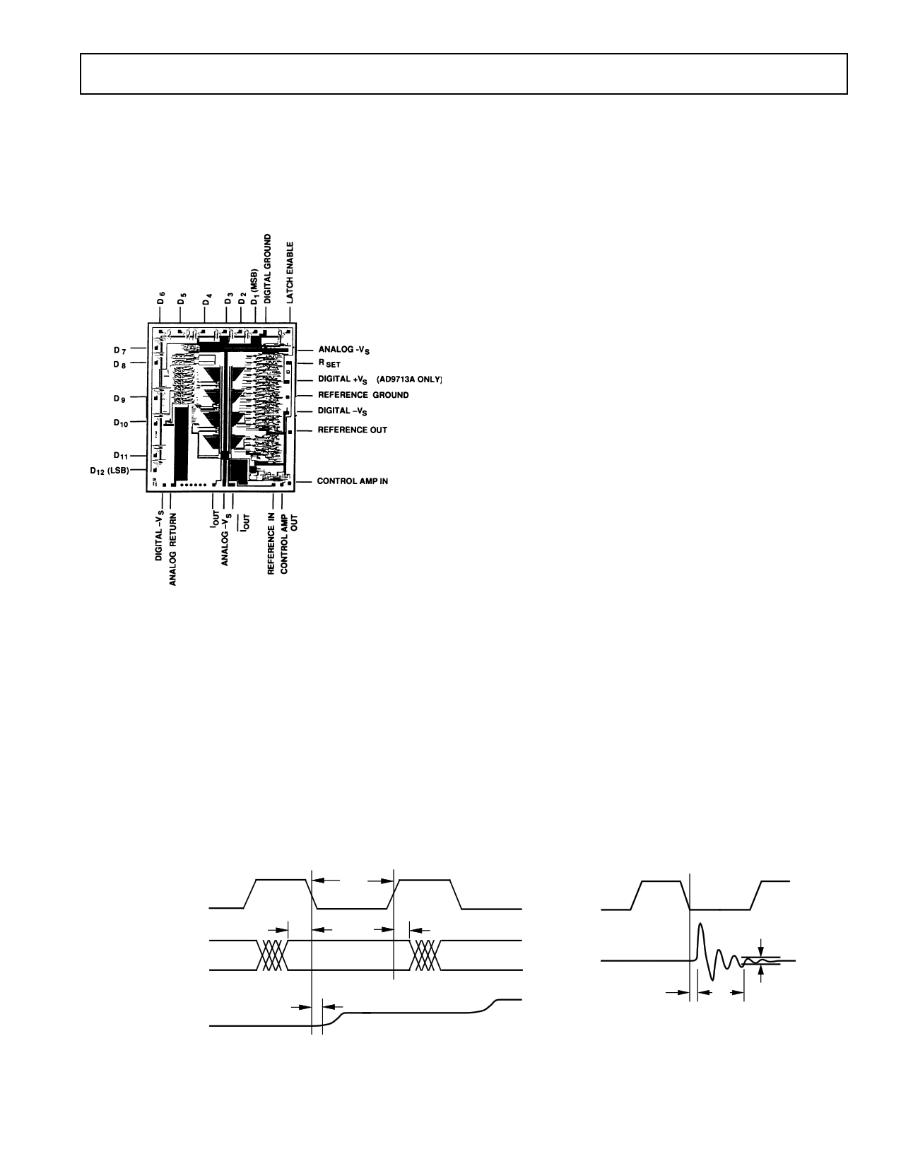
DIE LAYOUT AND METALIZATION INFORMATION
Die Dimensions . . . . . . . . . . . . . . . . . 220 × 196 × 15 (± 2) mils
Pad Dimensions . . . . . . . . . . . . . . . . . . . . . . . . . . . . . 4 × 4 mils
Metalization . . . . . . . . . . . . . . . . . . . . . . . . . . . . . . . Aluminum
Backing . . . . . . . . . . . . . . . . . . . . . . . . . . . . . . . . . . . . . . None
Substrate Potential . . . . . . . . . . . . . . . . . . . . . . . . . . . . . . . –VS
Passivation . . . . . . . . . . . . . . . . . . . . . . . . . . . . . . . . . . . Nitride
THEORY AND APPLICATIONS
The AD9712B and AD9713B high speed digital-to-analog
converters utilize Most Significant Bit (MSB) decoding and
segmentation techniques to reduce glitch impulse and main-
tain 12-bit linearity without trimming.
As shown in the functional block diagram, the design is based
on four main subsections: the Decoder/Driver circuits, the
Transparent Latches, the Switch Network, and the Control Am-
plifier. An internal bandgap reference is also included to allow
operation with a minimum of external components.
Digital Inputs/Timing
The AD9712B employs single-ended ECL-compatible inputs
for data inputs D1–D12 and LATCH ENABLE. The internal
ECL midpoint reference is designed to match 10K ECL device
thresholds. On the AD9713B, a TTL translator is added at each
input; with this exception, the AD9712B and AD9713B are
identical.
In the Decoder/Driver section, the four MSBs (D1–D4) are
decoded to 15 “thermometer code” lines. An equalizing delay is
included for the eight Least Significant Bits (LSBs) and
LATCH ENABLE. This delay minimizes data skew, and data
setup and hold times at the latch inputs; this is important when
operating the latches in the transparent mode. Without the
delay, skew caused by the decoding circuits would degrade
glitch impulse.
The latches operate in their transparent mode when LATCH
ENABLE (Pin 26) is at logic level “0.” The latches should be
used to synchronize data to the current switches by applying a
narrow LATCH ENABLE pulse with proper data setup and
hold times as shown in the Timing Diagram. An external latch
at each data input, clocked out of phase with the Latch Enable,
operates the AD9712B/AD9713B in a master slave (edge-
triggered) mode. This is the optimum way to operate the DAC
because data is always stable at the DAC input. An external
latch eases timing constraints when using the converter.
Although the AD9712B/AD9713B chip is designed to provide
isolation from digital inputs to the outputs, some coupling of
digital transitions is inevitable, especially with TTL or CMOS
inputs applied to the AD9713B. Digital feedthrough can be re-
duced by forming a low-pass filter using a (200 Ω) series resistor
in series with the capacitance of each digital input; this rolls off
the slew rate of the digital inputs.
References
As shown in the functional block diagram, the internal bandgap
reference, control amplifier, and reference input are pinned out
for maximum user flexibility when setting the reference.
When using the internal reference, REFERENCE OUT (Pin 20)
should be connected to CONTROL AMP IN (Pin 19). CON-
TROL AMP OUT (Pin 18) should be connected to REFER-
ENCE IN (Pin 17) through a 20 Ω resistor. A 0.1 µF ceramic
capacitor from Pin 17 to –VS (Pin 15) improves settling by
decoupling switching noise from the current sink base line. A
reference current cell provides feedback to the control amp by
sinking current through RSET (Pin 24).
LATCH ENABLE
DATA INPUTS
OUTPUT
tS
t PD
t LPW
VALID DATA
tH
t LPW – LATCH PULSE WIDTH
tS – INPUT SETUP TIME
Timing Diagram
LATCH
ENABLE
OUTPUT
ERROR
ERROR
BAND
t PD tST
t H – INPUT HOLD TIME
tST – OUTPUT SETTLING TIME
t PD – OUTPUT PROPAGATION DELAY
REV. B
–5–
5 Page 
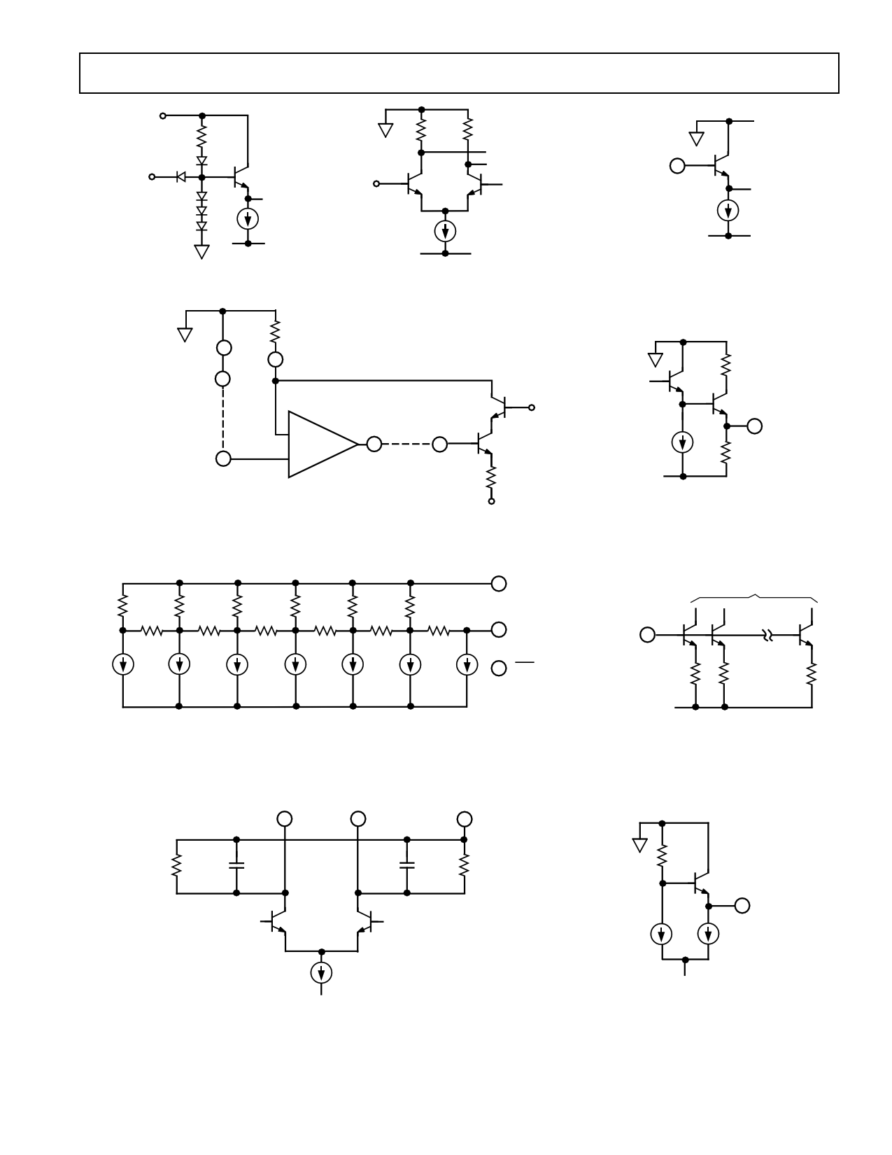
+5V
TTL
IN
10 kΩ
TTL Input Buffer
AD9712B/AD9713B
ECL
IN
ECL VMID
–5.2 V
ECL Input Buffer
CONTROL
AMP IN 19
–5.2 V
Control Amplifier Input
±
REFERENCE 20
OUT
24 R SET
CONTROL 19
AMP IN
+
CONTROL
AMP
–
18
CONTROL
AMP OUT
17
REFERENCE
IN
Full-Scale Current Control Loop
–5.2 V
VBIAS
–5.2 V
18 CONTROL
AMP OUT
Control Amp Output
R
R
2R
R
2R
R
2R
R
2R
R
2R
R
D12 D11
D10
D9
D 8 D7 D1– D 6
R-2R DAC (for 6 LSBs)
13 ANALOG
RETURN
138 CURRENT SOURCES
14 I OUT
or
16 I OUT
REFERENCE
IN
17
–5.2 V
Reference Input
I OUT
14
I OUT
16
ANALOG
RETURN
13
2.5kΩ
16pF
16pF
2.5kΩ
20 REFERENCE
OUT
REV. B
–VS
Output Circuit
Figure 11. Equivalent Circuits
–11–
–5.2 V
Reference Output
11 Page | ||
| Páginas | Total 12 Páginas | |
| PDF Descargar | [ Datasheet AD9712B.PDF ] | |
Hoja de datos destacado
| Número de pieza | Descripción | Fabricantes |
| AD9712 | 100MSPS D/A CONVERTERS | Analog Devices |
| AD9712B | 12-Bit/ 100 MSPS D/A Converters | Analog Devices |
| Número de pieza | Descripción | Fabricantes |
| SLA6805M | High Voltage 3 phase Motor Driver IC. |
Sanken |
| SDC1742 | 12- and 14-Bit Hybrid Synchro / Resolver-to-Digital Converters. |
Analog Devices |
|
DataSheet.es es una pagina web que funciona como un repositorio de manuales o hoja de datos de muchos de los productos más populares, |
| DataSheet.es | 2020 | Privacy Policy | Contacto | Buscar |
