|
|
PDF AD9283 Data sheet ( Hoja de datos )
| Número de pieza | AD9283 | |
| Descripción | 3V A/D Converter | |
| Fabricantes | Analog Devices | |
| Logotipo |  |
|
Hay una vista previa y un enlace de descarga de AD9283 (archivo pdf) en la parte inferior de esta página. Total 13 Páginas | ||
|
No Preview Available !
a
FEATURES
8-Bit, 50, 80, and 100 MSPS ADC
Low Power: 90 mW at 100 MSPS
On-Chip Reference and Track/Hold
475 MHz Analog Bandwidth
SNR = 46.5 dB @ 41 MHz at 100 MSPS
1 V p-p Analog Input Range
Single 3.0 V Supply Operation (2.7 V–3.6 V)
Power-Down Mode: 4.2 mW
APPLICATIONS
Battery Powered Instruments
Hand-Held Scopemeters
Low Cost Digital Oscilloscopes
8-Bit, 50 MSPS/80 MSPS/100 MSPS
3 V A/D Converter
AD9283
FUNCTIONAL BLOCK DIAGRAM
AIN
AIN
ENCODE
VD PWRDWN VDD
AD9283
T/H
ADC
OUTPUT
STAGING
TIMING
REF
8
D7–D0
GND
REF REF
OUT IN
GENERAL DESCRIPTION
The AD9283 is an 8-bit monolithic sampling analog-to-digital
converter with an on-chip track-and-hold circuit and is opti-
mized for low cost, low power, small size and ease of use. The
product operates at a 100 MSPS conversion rate, with outstand-
ing dynamic performance over its full operating range.
The ADC requires only a single 3.0 V (2.7 V to 3.6 V) power
supply and an encode clock for full performance operation. No
external reference or driver components are required for many
applications. The digital outputs are TTL/CMOS compatible
and a separate output power supply pin supports interfacing
with 3.3 V or 2.5 V logic.
The encoder input is TTL/CMOS compatible. A power-down
function may be exercised to bring total consumption to
4.2 mW. In power-down mode, the digital outputs are driven
to a high impedance state.
Fabricated on an advanced CMOS process, the AD9283 is
available in a 20-lead surface mount plastic package (SSOP)
specified over the industrial temperature range (–40°C to +85°C).
REV. C
Information furnished by Analog Devices is believed to be accurate and
reliable. However, no responsibility is assumed by Analog Devices for its
use, nor for any infringements of patents or other rights of third parties that
may result from its use. No license is granted by implication or otherwise
under any patent or patent rights of Analog Devices.
One Technology Way, P.O. Box 9106, Norwood, MA 02062-9106, U.S.A.
Tel: 781/329-4700
www.analog.com
Fax: 781/326-8703
© Analog Devices, Inc., 2001
1 page 
AD9283
EXPLANATION OF TEST LEVELS
Test Level
I 100% production tested.
II 100% production tested at 25°C and sample tested at
specified temperatures.
III Sample tested only.
IV Parameter is guaranteed by design and characteriza-
tion testing.
V Parameter is a typical value only.
VI 100% production tested at 25°C; guaranteed by design and
characterization testing for industrial temperature range;
100% production tested at temperature extremes for mili-
tary devices.
Step
255
•
•
128
127
•
•
0
Table I. Output Coding (VREF = 1.25 V)
AIN–AIN
0.512
•
•
0.002
–0.002
•
•
–0.512
Digital Output
1111 1111
•
•
1000 0000
0111 1111
•
•
0000 0000
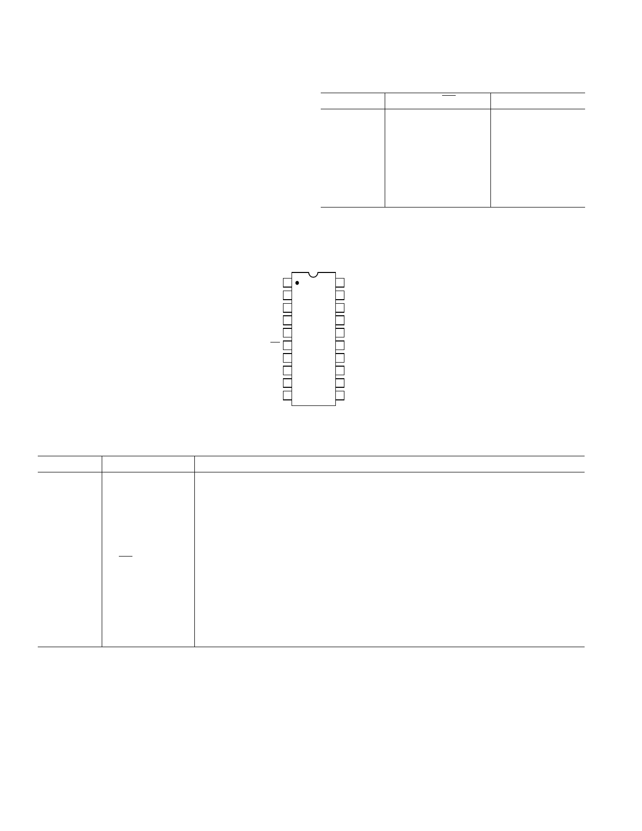
PIN CONFIGURATION
PWRDWN 1
20 D0 (LSB)
VREF OUT 2
19 D1
VREF IN 3
18 D2
GND 4
17 D3
VD 5 AD9283 16 GND
A IN
6
TOP VIEW
(Not to Scale)
15
VDD
AIN 7
14 D4
VD 8
13 D5
GND 9
12 D6
ENCODE 10
11 D7 (MSB)
Pin Number
1
2
3
4, 9, 16
5, 8
6
Mnemonic
PWRDWN
VREF OUT
VREF IN
GND
VD
AIN
7
10
11–14, 17–20
15
AIN
ENCODE
D7–D4, D3–D0
VDD
PIN FUNCTION DESCRIPTIONS
Function
Power-Down Function Select; Logic HIGH for Power-Down Mode (Digital Outputs Go
to High Impedance State)
Internal Reference Output (1.25 V typ); Bypass with 0.1 µF to Ground
Reference Input for ADC (1.25 V typ)
Ground
Analog 3 V Power Supply
Analog Input for ADC (Can Be Left Open if Operating in Single-Ended Mode, but Rec-
ommend Connection to a 0.1 µF Capacitor and a 25 Ω Resistor in Series to Ground for
Better Input Matching)
Analog Input for ADC
Encode Clock for ADC (ADC Samples on Rising Edge of ENCODE)
Digital Outputs of ADC
Digital output power supply. Nominally 2.5 V to 3.6 V
–4– REV. C
5 Page 
AD9283
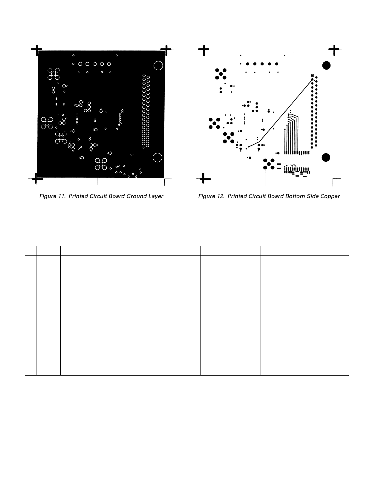
Figure 11. Printed Circuit Board Ground Layer
Figure 12. Printed Circuit Board Bottom Side Copper
# Qty
1 15
24
3 24
44
51
61
75
81
91
10 1
11 1
12 1
13 1
14 1
EVALUATION BOARD BILL OF MATERIALS — GS01717
REFDES
C1, C4–C17
C18–C21
E1–E6, E8–E10, E12–E19,
E21, E34–E39
J1, J2, J3, J5
P1
Device
Ceramic Cap
Tantalum Cap
W-HOLE
Connector
5-Pin Connector
Package
0603
BCAPTAJD
SMB
P2
R4, R9, R10, R21, R22
R7
R23
T1
U1
U3
U4
U5
37-Pin Connector
Resistor
Resistor
Resistor
Transformer
AD9283
AD9760
74ACQ574
SN74LVC86
1206
1206
1206
SSOP-20
SOIC-28
SOIC-20
SO14
Value
0.1 µF
10 µF
Wieland Connector
(P/N #25.602.2553.0 Top
P/N #Z5.530.0525.0 Bottom)
AMP-747462-2
50 Ω
25 Ω
2 kΩ
Mini-Circuits T1-1T-KK81
–10–
REV. C
11 Page | ||
| Páginas | Total 13 Páginas | |
| PDF Descargar | [ Datasheet AD9283.PDF ] | |
Hoja de datos destacado
| Número de pieza | Descripción | Fabricantes |
| AD9280 | CMOS A/D Converter | Analog Devices |
| AD9281 | Dual Channel 8-Bit Resolution CMOS ADC | Analog Devices |
| AD9283 | 3V A/D Converter | Analog Devices |
| AD9284 | 1.8 V Dual Analog-to-Digital Converter (ADC) | Analog Devices |
| Número de pieza | Descripción | Fabricantes |
| SLA6805M | High Voltage 3 phase Motor Driver IC. |
Sanken |
| SDC1742 | 12- and 14-Bit Hybrid Synchro / Resolver-to-Digital Converters. |
Analog Devices |
|
DataSheet.es es una pagina web que funciona como un repositorio de manuales o hoja de datos de muchos de los productos más populares, |
| DataSheet.es | 2020 | Privacy Policy | Contacto | Buscar |
