|
|
|
PDF AD9070 Data sheet ( Hoja de datos )
| Número de pieza | AD9070 | |
| Descripción | 10-Bit 100 MSPS A/D Converter | |
| Fabricantes | Analog Devices | |
| Logotipo | ||
Hay una vista previa y un enlace de descarga de AD9070 (archivo pdf) en la parte inferior de esta página. Total 16 Páginas | ||
|
No Preview Available !
a
10-Bit, 100 MSPS
A/D Converter
AD9070
FEATURES
10-Bit, 100 MSPS ADC
Low Power: 600 mW Typical at 100 MSPS
On-Chip Track/Hold
230 MHz Analog Bandwidth
SINAD = 54 dB @ 41 MHz
On-Chip Reference
1 V p-p Analog Input Range
Single Supply Operation: +5 V or –5 V
Differential Clock Input
Available in Standard Military Drawing Version
APPLICATIONS
Digital Communications
Signal Intelligence
Digital Oscilloscopes
Spectrum Analyzers
Medical Imaging
Radar
HDTV
GENERAL DESCRIPTION
The AD9070 is a monolithic sampling analog-to-digital
converter with an on-chip track-and-hold circuit and ECL
digital interfaces. The product operates at a 100 MSPS
conversion rate with outstanding dynamic performance over
its full operating range.
The ADC requires only a single –5 V supply and an encode
clock for full performance operation. The digital outputs are
ECL compatible, while a differential clock input accommodates
a wide range of logic levels. The AD9070 may be operated in a
Positive ECL (PECL) environment with a single +5 V supply.
An Out-of-Range output (OR) is available in the DIP version to
indicate that a conversion result is outside the operating range.
In both package styles, the output data are held at saturation
levels during an out-of-range condition.
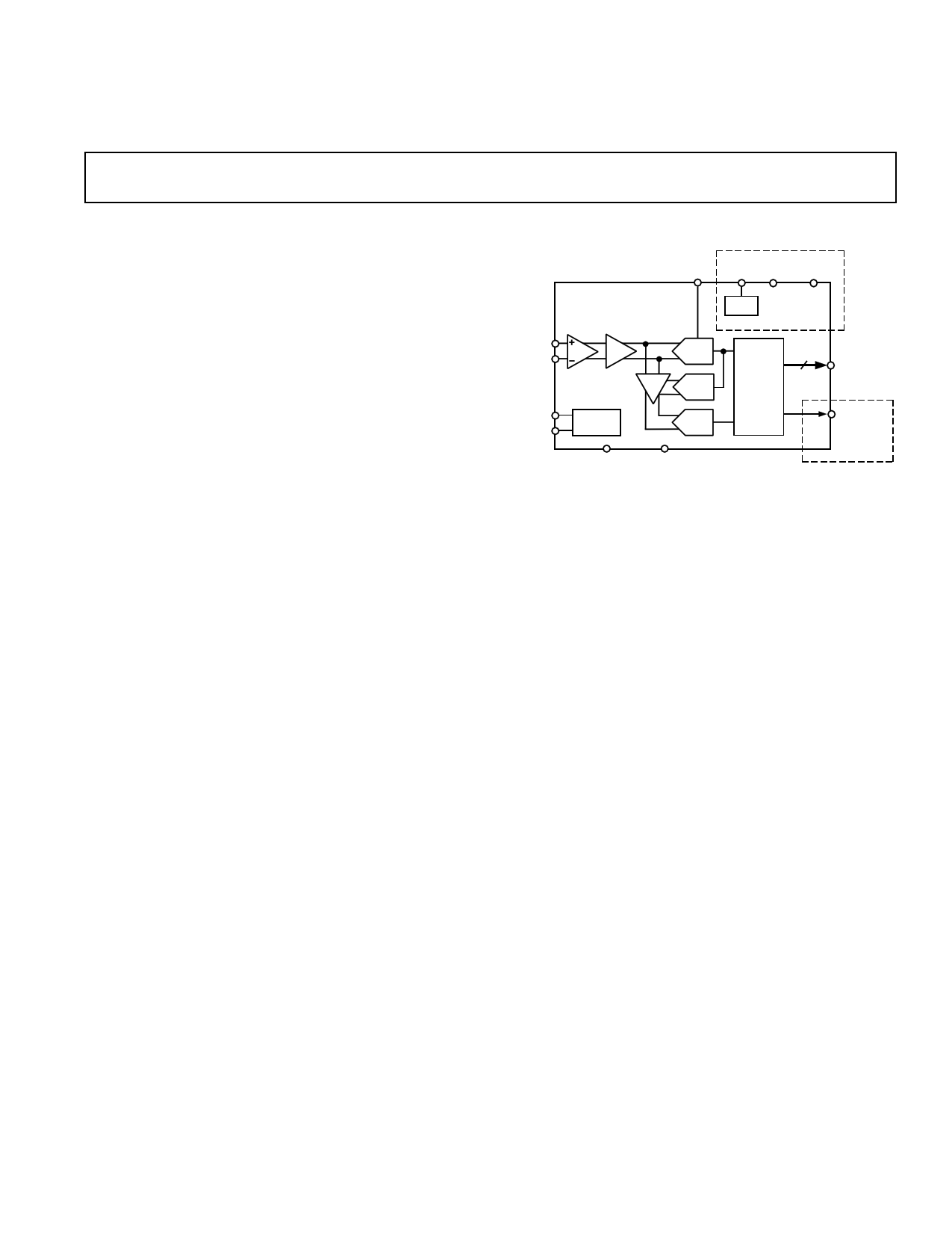
FUNCTIONAL BLOCK DIAGRAM
AIN
AIN
ENCODE
ENCODE
AD9070
VREF VREF
REF
IN OUT COMP BYPASS
–2.5V
SOIC (BR)
PACKAGE
ONLY
T/H
SUM
AMP
TIMING
ADC
DAC
ADC
VEE GND
10
ENCODE
LOGIC
D9 – D0
OR
DIP
PACKAGE
ONLY
The input amplifier supports single-ended interfaces. An
internal –2.5 V reference is included in the SOIC packaged
device (an external voltage reference is required for the
DIP version).
Fabricated on an advanced bipolar process, the AD9070
is available in a plastic SOIC package specified over the
industrial temperature range (–40°C to +85°C), and a full
MIL-PRF-38534 QML version (–55°C to +125°C) in a
ceramic Dual-in-Line Package (DIP).
REV. C
Information furnished by Analog Devices is believed to be accurate and
reliable. However, no responsibility is assumed by Analog Devices for its
use, nor for any infringements of patents or other rights of third parties that
may result from its use. No license is granted by implication or otherwise
under any patent or patent rights of Analog Devices.
One Technology Way, P.O. Box 9106, Norwood, MA 02062-9106, U.S.A.
Tel: 781/329-4700
www.analog.com
Fax: 781/326-8703
© Analog Devices, Inc., 2001
1 page 
AD9070
PIN FUNCTION DESCRIPTIONS
Pin Numbers
AD9070BR
AD9070DIP
R Package
D Package
Mnemonic Function
1, 7, 12, 21, 23
2, 8, 11, 20, 22
3
4
5
6
9
10
13
14
28–24, 19–15
N/A
1, 7, 9, 14, 21
2, 6, 8, 10, 13, 15, 22
N/A
3
N/A
N/A
4
5
11
12
27–23, 20–16
28
VEE
GND
VREF OUT
VREF IN
COMP
REF BYPASS
AIN
AIN
ENCODE
ENCODE
D9–D0
OR
Negative Power Supply. Nominally –5.0 V.
Ground
Internal Reference Output (–2.5 V typical); Bypass with 0.1 µF to Ground
Reference Input for ADC (–2.5 V typical)
Internal Amplifier Compensation, 0.1 µF to VEE
Reference Bypass Node, 0.1 µF to VEE
Analog Input – Complement
Analog Input – True
Encode Clock for ADC (ADC Samples on Rising Edge of ENCODE).
Encode Clock Complement (ADC Samples on Falling Edge of ENCODE).
Digital Outputs of ADC. D9 is the MSB. Data is two’s complement.
Out-of-Range Output. Goes HIGH when the converted sample is more
positive than 1FFh or more negative than 200h (Two’s Complement Coding).
SOIC
PIN CONFIGURATIONS
Ceramic DIP
VEE 1
GND 2
28 D9 (MSB)
27 D8
VREF OUT 3
26 D7
VREF IN 4
25 D6
COMP 5
24 D5
REF BYPASS 6 AD9070BR 23 VEE
VEE 7 TOP VIEW 22 GND
(Not to Scale)
GND 8
21 VEE
AIN 9
20 GND
AIN 10
19 D4
GND 11
18 D3
VEE 12
ENCODE 13
ENCODE 14
17 D2
16 D1
15 D0 (LSB)
VEE 1
GND 2
28 OR
27 D9 (MSB)
VREF IN 3
AIN 4
26 D8
25 D7
AIN 5
24 D6
GND 6 AD9070DIP 23 D5
VEE 7 TOP VIEW 22 GND
(Not to Scale)
GND 8
21 VEE
VEE 9
20 D4
GND 10
19 D3
ENCODE 11
ENCODE 12
18 D2
17 D1
GND 13
16 D0 (LSB)
VEE 14
15 GND
REV. C
–5–
5 Page 
AD9070
5 V Operation
The AD9070 may be operated above ground, with a single 5 V
power supply. All power supply ground pins are connected to
5 V, and VEE pins are connected to ground (Figure 12). Care must
be taken in connecting signals and determining bypass rails.
The reference voltage (REF OUT) is still generated with respect
to the positive rail, which is now 5 V. It is nominally 2.5 V, but
its voltage with respect to ground will vary directly with changes
in the power supply voltage (for example, if the power supply
goes to 5.1 V, the reference becomes 2.6 V). The reference
input is likewise processed with respect to 5 V. This dictates
that these pins be bypassed to 5 V as well. However, the COMP
and REF BYPASS pins must continue to be bypassed to the
most negative supply, which is now ground. The AIN input
must still be connected or bypassed to the ground reference of
the input signal.
Package Options
The AD9070 is available in two packages. The BR package is a
standard 28-lead Small Outline IC (SOIC). The DIP package is
a ceramic Dual-in-Line Hybrid. The SOIC is offered in a commer-
cial grade, and specified over the industrial (–40°C to +85°C)
temperature range. The DIP is a full MIL-PRF-38534 QML
version that operates from (–55°C to +125°C).
The SOIC version includes the on-chip voltage reference, whereas
the DIP does not. The DIP, however, provides the Overrange
(OR) output, and includes reference and power supply bypass-
ing, along with an internal compensation capacitor.
Equivalent performance may be obtained with either part though,
due to the internal bypassing, the DIP is not as sensitive to
board layout and parasitics.
5V
VIN
1Vp-p
0.1F
RT 500⍀
0.1F
10H
0.1F
GND
AIN
AD9070
AIN
(MSB) D9
VREF OUT
VREF IN
D9
510⍀
(OR 100⍀ TO +3V)
ENCODE
ENCODE
5V (LSB) D0
ENCODE
ENCODE
REF
COMP VEE BYPASS
D0
510⍀
(OR 100⍀ TO +3V)
0.1F
0.1F
Figure 12. AD9070 in 5 V (PECL) Environment
REV. C
–11–
11 Page | ||
| Páginas | Total 16 Páginas | |
| PDF Descargar | [ Datasheet AD9070.PDF ] | |
Hoja de datos destacado
| Número de pieza | Descripción | Fabricantes |
| AD9070 | 10-Bit 100 MSPS A/D Converter | Analog Devices |
| AD9071 | 10-Bit 100 MSPS A/D Converter | Analog Devices |
| Número de pieza | Descripción | Fabricantes |
| SLA6805M | High Voltage 3 phase Motor Driver IC. |
Sanken |
| SDC1742 | 12- and 14-Bit Hybrid Synchro / Resolver-to-Digital Converters. |
Analog Devices |
|
DataSheet.es es una pagina web que funciona como un repositorio de manuales o hoja de datos de muchos de los productos más populares, |
| DataSheet.es | 2020 | Privacy Policy | Contacto | Buscar |