|
|
|
PDF AD9054A Data sheet ( Hoja de datos )
| Número de pieza | AD9054A | |
| Descripción | 8-Bit / 200 MSPS A/D Converter | |
| Fabricantes | Analog Devices | |
| Logotipo | ||
Hay una vista previa y un enlace de descarga de AD9054A (archivo pdf) en la parte inferior de esta página. Total 20 Páginas | ||
|
No Preview Available !
a
FEATURES
200 MSPS Guaranteed Conversion Rate
135 MSPS Low Cost Version Available
350 MHz Analog Bandwidth
1 V p-p Analog Input Range
Internal 2.5 V Reference and T/H
Low Power: 500 mW
5 V Single Supply Operation
TTL Output Interface
Single or Demultiplexed Output Ports
APPLICATIONS
RGB Graphics Processing
High Resolution Video
Digital Data Storage Read Channels
Digital Communications
Digital Instrumentation
Medical Imaging
8-Bit, 200 MSPS
A/D Converter
AD9054A
AIN
AIN
ENCODE
ENCODE
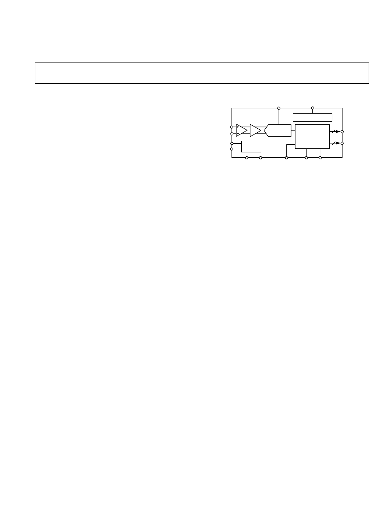
FUNCTIONAL BLOCK DIAGRAM
VREF IN
VREF OUT
AD9054A
2.5V REFERENCE
T/H
TIMING
QUANTIZER
8
ENCODE
LOGIC
DEMULTIPLEXER 8
DA7 – D A0
DB7 – D B0
VDD GND
DEMUX
DS DS
GENERAL DESCRIPTION
The AD9054A is an 8-bit monolithic analog-to-digital converter
optimized for high speed, low power, small size and ease of use.
With a 200 MSPS encode rate capability and full-power analog
bandwidth of 350 MHz, the component is ideal for applications
requiring the highest possible dynamic performance.
To minimize system cost and power dissipation, the AD9054A
includes an internal 2.5 V reference and track-and-hold circuit.
The user provides only a 5 V power supply and an encode clock.
No external reference or driver components are required for
many applications.
The AD9054A’s encode input interfaces directly to TTL, CMOS
or positive-ECL logic and will operate with single-ended or
differential inputs. The user may select dual-channel or single-
channel digital outputs. The dual (demultiplexed) mode inter-
leaves ADC data through two 8-bit channels at one-half the
clock rate. Operation in demultiplexed mode reduces the speed
and cost of external digital interfaces while allowing the ADC to
be clocked to the full 200 MSPS conversion rate. In the single-
channel (nondemultiplexed) mode, all data is piped at the full
clock rate to the Channel A outputs.
Fabricated with an advanced BiCMOS process, the AD9054A is
provided in a space-saving 44-lead LQFP surface mount plastic
package (ST-44) and specified over the full industrial (–40°C to
+85°C) temperature range.
REV. D
Information furnished by Analog Devices is believed to be accurate and
reliable. However, no responsibility is assumed by Analog Devices for its
use, nor for any infringements of patents or other rights of third parties that
may result from its use. No license is granted by implication or otherwise
under any patent or patent rights of Analog Devices.
One Technology Way, P.O. Box 9106, Norwood, MA 02062-9106, U.S.A.
Tel: 781/329-4700
www.analog.com
Fax: 781/326-8703
© Analog Devices, Inc., 2001
1 page 
PIN FUNCTION DESCRIPTIONS
Pin Number Mnemonic Function
1
2
3, 5, 15, 18, 28,
30, 31, 36, 41
4, 6, 16, 17, 27,
29, 32, 35, 37, 40
14–7
19–26
33
34
38
39
42
43
44
ENCODE
ENCODE
VDD
GND
DA0–DA7
DB0–DB7
VREF OUT
VREF IN
AIN
AIN
DEMUX
DS
DS
Encode Clock for ADC (ADC
Samples on Rising Edge
of ENCODE)
Encode Clock Complement
(ADC Samples on Falling Edge
of ENCODE)
Power Supply (5 V)
Ground
Digital Outputs of ADC Channel
A. DA7 is the MSB, DA0 the LSB
Digital Outputs of ADC Channel
B. DB7 is the MSB, DB0 the LSB
Internal Reference Output
(2.5 V typical); Bypass with
0.1 µF to Ground
Reference Input for ADC (2.5 V
typical, ± 4%)
Analog Input—Complement.
Connect to input signal midscale
reference.
Analog Input—True
Format Select. LOW = Dual.
Channel Mode, HIGH = Single.
Channel Mode (Channel A Only)
Data Sync Complement
Data Sync—Aligns Output Chan-
nels in Dual-Channel Mode
AD9054A
PIN CONFIGURATION
VREF IN
GND
VDD
GND
AIN
AIN
GND
VDD
DEMUX
DS
DS
AD9054A
TOP VIEW
(PINS DOWN)
PIN 1
IDENTIFIER
DB3
DB2
DB1
DB0 (LSB)
VDD
GND
GND
VDD
DA0 (LSB)
DA1
DA2
SAMPLE N–1
SAMPLE N
SAMPLE N+3
SAMPLE N+4
AIN
ENCODE
ENCODE
D7 – D 0
tA
tEH
SAMPLE N+1
tEL 1/fS
SAMPLE N+2
DATA N–5
DATA N–4
DATA N–3
DATA N–2
tPD
tV
DATA N–1
DATA N
Figure 1. Timing—Single Channel Mode
REV. D
–5–
5 Page 
0
–10 F1 = 55.0MHz
F2 = 56.0MHz
–20 F1 = F2 = –7.0dBFS
–30
–40
–50
–60
–70
–80
–90
–100
0
10 20 30 40 50 60 70 80 90 100
MHz
TPC 19. Two-Tone Intermodulation Distortion
5.0
4.5
4.0
3.5
3.0
2.5
2.0
1.5
1.0
0.5
0.0
0.0 –1.0 –2.0 –3.0 –4.0 –5.0 –6.0 –7.0 –8.0 –9.0 –10.0
IOH – mA
TPC 20. Output Voltage HIGH vs. Output Current
1.0
0.9
0.8
0.7
0.6
0.5
0.4
0.3
0.2
0.1
0.0
0.0 1.0 2.0 3.0 4.0 5.0 6.0 7.0 8.0
IOL – mA
TPC 21. Output Voltage LOW vs. Output Current
AD9054A
7
tPD
6
tV
5
4
3
2
1
0
–60 –40 –20 0 20 40 60 80 100
TC – ؇C
TPC 22. Output Delay vs. Temperature
2.55
2.54
2.53
2.52
2.51
2.50
2.49
2.48
2.47
2.46
2.45
–20 –18 –16 –14 –12 –10 –8 –6 –4 –2 0 2
IREF OUT – mA
TPC 23. Reference Voltage vs. Reference Load
2.502
2.501
2.500
2.499
2.498
3.0
3.5
4.0 4.5
5.0 5.5
6.0 6.5
VDD – Volts
TPC 24. Reference Voltage vs. Power Supply Voltage
REV. D
–11–
11 Page | ||
| Páginas | Total 20 Páginas | |
| PDF Descargar | [ Datasheet AD9054A.PDF ] | |
Hoja de datos destacado
| Número de pieza | Descripción | Fabricantes |
| AD9054 | 8-Bit/ 200 MSPS A/D Converter | Analog Devices |
| AD9054A | 8-Bit / 200 MSPS A/D Converter | Analog Devices |
| Número de pieza | Descripción | Fabricantes |
| SLA6805M | High Voltage 3 phase Motor Driver IC. |
Sanken |
| SDC1742 | 12- and 14-Bit Hybrid Synchro / Resolver-to-Digital Converters. |
Analog Devices |
|
DataSheet.es es una pagina web que funciona como un repositorio de manuales o hoja de datos de muchos de los productos más populares, |
| DataSheet.es | 2020 | Privacy Policy | Contacto | Buscar |