|
|
|
PDF AD8598 Data sheet ( Hoja de datos )
| Número de pieza | AD8598 | |
| Descripción | Dual 7 ns Single Supply Comparator | |
| Fabricantes | Analog Devices | |
| Logotipo | ||
Hay una vista previa y un enlace de descarga de AD8598 (archivo pdf) en la parte inferior de esta página. Total 11 Páginas | ||
|
No Preview Available !
a
FEATURES
7 ns Propagation Delay
Single Supply Operation: +3 V to +10 V
Low Power
Symmetrical Layout
Latch Function
TSSOP Packages
APPLICATIONS
Clock Recovery and Clock Distribution
High Speed Data
Line Receivers
Phase Detectors
Digital Communications
I and Q Detection
High Speed Sampling
Upgrade for MAX912
Satellite Receivers
PCMCIA Cards
Wireless Data Links
Battery Operated Instrumentation
GENERAL DESCRIPTION
The AD8598 is a dual 7 ns comparator with digital latches.
Separate supplies enable the input stage to be operated from
+5 V to as high as ± 5 V.
Ultrafast 7 ns propagation delay makes the AD8598 a good
choice for timing circuits and line receivers. Propagation delays
for rising and falling signals are closely matched and track over
temperature. This matched delay makes the AD8598 a good
choice for clock recovery, since the duty cycle of the output will
match the duty cycle of the input.
The AD8598 has the same pinout as the DIP version of the
AD9698. For a single comparator like the AD8598, please refer
to the AD8561 data sheet.
The AD8598 is specified over the industrial (–40°C to +85°C)
temperature range. The AD8598 is available in both the 16-lead
plastic DIP, 16-lead TSSOP or narrow R-16A surface mount
packages.
Dual 7 ns
Single Supply Comparator
AD8598
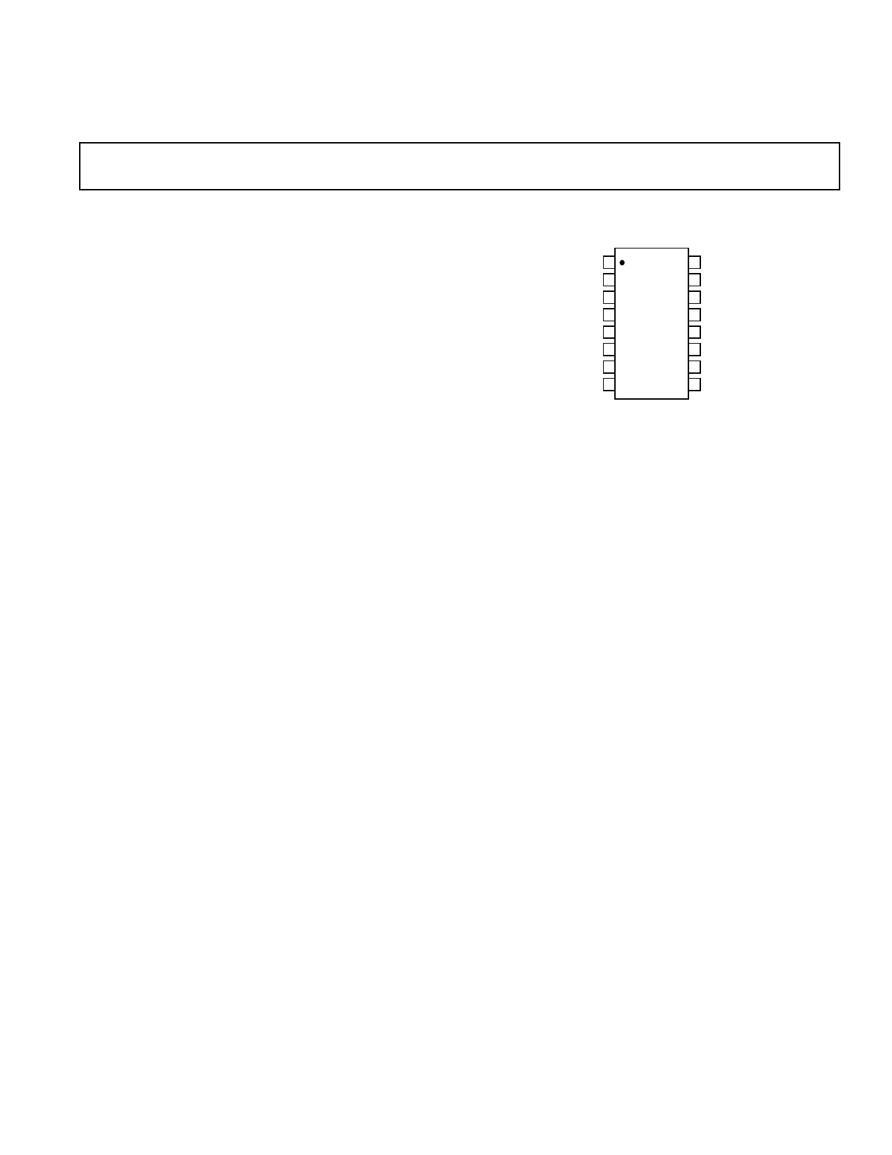
PIN CONFIGURATIONS
N-16, RU-16 and R-16A
QA 1
QA 2
GND 3
LEA 4
NC 5
V– 6
IN A– 7
IN A+ 8
16 QB
15 QB
AD8598
TOP VIEW
(Not to Scale)
14 GND
13 LEB
12 NC
11 V+
10 IN B–
9 IN B+
NC = NO CONNECT
REV. A
Information furnished by Analog Devices is believed to be accurate and
reliable. However, no responsibility is assumed by Analog Devices for its
use, nor for any infringements of patents or other rights of third parties
which may result from its use. No license is granted by implication or
otherwise under any patent or patent rights of Analog Devices.
One Technology Way, P.O. Box 9106, Norwood, MA 02062-9106, U.S.A.
Tel: 781/329-4700 World Wide Web Site: http://www.analog.com
Fax: 781/326-8703
© Analog Devices, Inc., 1998
1 page 
AD8598
Typical Performance Characteristics (V+ = +5 V, V– = 0 V, TA = +25؇C unless otherwise noted)
5
+125؇C
4
VS = +5V, SINGLE SUPPLY
؊40؇C
3
+25؇C
2
500
400
300
200
20
VS = +5V, SINGLE SUPPLY
STEP SIZE = 100mV
CAPACITANCE LOAD = 10pF
15
TA = +25؇C
10
1 100
5
0
؊2.5 ؊2.0 ؊1.5 ؊1.0 ؊0.5 0 0.5 1.0 1.5
DIFFERENTIAL INPUT VOLTAGE – mV
Figure 1. Output Voltage vs. Differen-
tial Input Voltage
0
؊5 ؊4 ؊3 ؊2 ؊1 0 1 2 3 4 5
INPUT VOLTAGE – mV
Figure 2. Typical Distribution of Input
Offset Voltage
0
0
10
20 30
40
50
OVERDRIVE – mV
Figure 3. Propagation Delay vs.
Overdrive
20
VS = +5V, SINGLE SUPPLY
STEP SIZE = 100mV
OVERDRIVE LOAD = 5mV
15
tPD ؊
FALLING EDGE
10
tPD +
FALLING EDGE
5
0
0 10 20 30 40 50
LOAD CAPACITANCE – pF
Figure 4. Propagation Delay vs. Load
Capacitance
40
VS = +5V, SINGLE SUPPLY
OVERDRIVE = 10mV
TA = +25؇C
CAPACITANCE LOAD = 10pF
30
STEP SIZE = 800mV
200mV
20
400mV
100mV
10
20
SINGLE SUPPLY
STEP SIZE = 100mV
TA = +25؇C
15 OVERDRIVE = 5mV
CAPACITANCE LOAD = 10pF
10
5
0
0 0.5 1 1.5 2
SOURCE RESISTANCE – k⍀
Figure 5. Propagation Delay vs.
Source Resistance
0
4.5
4.75 5 5.25
SUPPLY VOLTAGE – Volts
5.5
Figure 6. Propagation Delay vs. Posi-
tive Supply Voltage
20
VS = +5V, SINGLE SUPPLY
STEP SIZE = 100mV
15 OVERDRIVE = 5mV,
LOAD CAPACITANCE = 10pF
10
5
0
–50 –25
0 25 50 75 100 125
TEMPERATURE – ؇C
Figure 7. Propagation Delay vs.
Temperature
20
+25؇C
15
؊40؇C
+125؇C
10
5 VS = +5V
STEP SIZE = 100mV
OVERDRIVE = 5mV
LOAD CAPACITANCE = 10pF
0
01
23
4
COMMON-MODE VOLTAGE – Volts
5
Figure 8. Propagation Delay vs. VCM
4
3
2 HOLD TIME
1
SETUP TIME
0
–50 –25
0 25 50 75
TEMPERATURE – ؇C
100 125
Figure 9. Latch Setup-and-Hold Time
vs. Temperature
REV. A
–5–
5 Page 
REV. A
OUTLINE DIMENSIONS
Dimensions shown in inches and (mm).
16-Lead Plastic DIP
(N-16)
0.840 (21.33)
0.745 (18.93)
16
1
PIN 1
0.210 (5.33)
MAX
0.160 (4.06)
0.115 (2.93)
0.022 (0.558)
0.014 (0.356)
0.100
(2.54)
BSC
9 0.280 (7.11)
0.240 (6.10)
8
0.060 (1.52)
0.015 (0.38)
0.325 (8.25)
0.300 (7.62) 0.195 (4.95)
0.115 (2.93)
0.130
(3.30)
MIN
0.070 (1.77) SEATING
0.045 (1.15) PLANE
0.015 (0.381)
0.008 (0.204)
16-Lead Thin Shrink Small Outline
(RU-16)
0.201 (5.10)
0.193 (4.90)
16
0.177 (4.50)
0.169 (4.30)
1
9
0.256 (6.50)
0.246 (6.25)
8
0.006 (0.15) PIN 1
0.002 (0.05)
0.0256 0.0118 (0.30)
SEATING (0.65)
PLANE BSC
0.0075 (0.19)
0.0433
(1.10)
MAX
0.0079 (0.20)
8؇
0؇
0.0035 (0.090)
0.028 (0.70)
0.020 (0.50)
16-Lead Narrow Body IC
(R-16A)
0.3937 (10.00)
0.3859 (9.80)
0.1574 (4.00) 16
0.1497 (3.80) 1
9
0.2440 (6.20)
8 0.2284 (5.80)
0.0098 (0.25)
0.0040 (0.10)
PIN 1
0.0688 (1.75)
0.0532 (1.35)
0.0196
0.0099
(0.50)
(0.25)
؋
45؇
SEATING
PLANE
0.0500
(1.27)
BSC
8؇
0.0192 (0.49)
0.0138 (0.35)
0.0099 (0.25) 0؇
0.0500 (1.27)
0.0075 (0.19) 0.0160 (0.41)
AD8598
–11–
11 Page | ||
| Páginas | Total 11 Páginas | |
| PDF Descargar | [ Datasheet AD8598.PDF ] | |
Hoja de datos destacado
| Número de pieza | Descripción | Fabricantes |
| AD8591 | Rail-to-Rail Input/Output Operational Amplifiers | Analog Devices |
| AD8592 | Rail-to-Rail Input/Output Operational Amplifiers | Analog Devices |
| AD8594 | Rail-to-Rail Input/Output Operational Amplifiers | Analog Devices |
| AD8597 | Ultralow Noise Op Amp | Analog Devices |
| Número de pieza | Descripción | Fabricantes |
| SLA6805M | High Voltage 3 phase Motor Driver IC. |
Sanken |
| SDC1742 | 12- and 14-Bit Hybrid Synchro / Resolver-to-Digital Converters. |
Analog Devices |
|
DataSheet.es es una pagina web que funciona como un repositorio de manuales o hoja de datos de muchos de los productos más populares, |
| DataSheet.es | 2020 | Privacy Policy | Contacto | Buscar |