|
|
|
PDF ADR420 Data sheet ( Hoja de datos )
| Número de pieza | ADR420 | |
| Descripción | Ultraprecision Low Noise/ 2.048 V/2.500 V/ 3.00 V/5.00 V XFET Voltage References | |
| Fabricantes | Analog Devices | |
| Logotipo | ||
Hay una vista previa y un enlace de descarga de ADR420 (archivo pdf) en la parte inferior de esta página. Total 16 Páginas | ||
|
No Preview Available !
a Ultraprecision Low Noise, 2.048 V/2.500 V/
3.00 V/5.00 V XFET® Voltage References
ADR420/ADR421/ADR423/ADR425
FEATURES
Low Noise (0.1 Hz to 10 Hz)
ADR420: 1.75 V p-p
ADR421: 1.75 V p-p
ADR423: 2.0 V p-p
ADR425: 3.4 V p-p
Low Temperature Coefficient: 3 ppm/؇C
Long-Term Stability: 50 ppm/1000 Hours
Load Regulation: 70 ppm/mA
Line Regulation: 35 ppm/V
Low Hysteresis: 40 ppm Typical
Wide Operating Range
ADR420: 4 V to 18 V
ADR421: 4.5 V to 18 V
ADR423: 5 V to 18 V
ADR425: 7 V to 18 V
Quiescent Current: 0.5 mA Maximum
High Output Current: 10 mA
Wide Temperature Range: –40؇C to +125؇C
APPLICATIONS
Precision Data Acquisition Systems
High-Resolution Converters
Battery-Powered Instrumentation
Portable Medical Instruments
Industrial Process Control Systems
Precision Instruments
Optical Network Control Circuits
GENERAL DESCRIPTION
The ADR42x series are ultraprecision second-generation XFET
voltage references featuring low noise, high accuracy, and excellent
long-term stability in a SOIC and Mini_SOIC footprints. Patented
temperature drift curvature correction technique and XFET (eXtra
implanted junction FET) technology minimize nonlinearity of the
voltage change with temperature. The XFET architecture offers
superior accuracy and thermal hysteresis to the bandgap
references. It also operates at lower power and lower supply
headroom than the Buried Zener references.
The superb noise, stable, and accurate characteristics of ADR42x
make them ideal for precision conversion applications such as
optical network and medical equipment. The ADR42x trim
terminal can also be used to adjust the output voltage over a
±0.5% range without compromising any other performance. The
ADR42x series voltage references offer two electrical grades and
are specified over the extended industrial temperature range
of –40°C to +125°C. Devices are available in 8-lead SOIC-8 or
30% smaller 8-lead Mini_SOIC-8 packages.
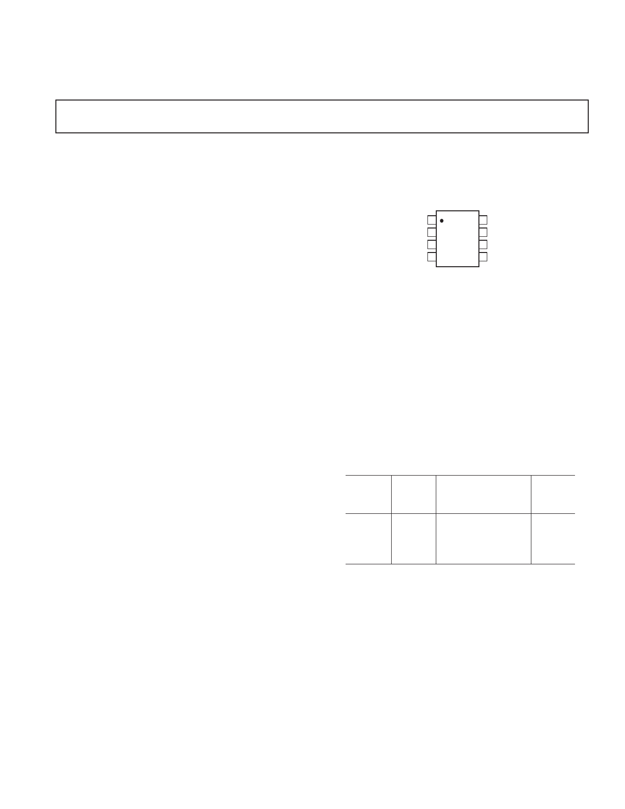
PIN CONFIGURATION
Surface-Mount Packages
8-Lead SOIC
8-Lead Mini_SOIC
TP 1
8 TP
VIN 2 ADR42x 7 NIC
NIC 3 TOP VIEW 6 VOUT
GND 4 (Not to Scale) 5 TRIM
NIC = NO INTERNAL CONNECTION
TP = TEST PIN (DO NOT CONNECT)
Table I. ADR42x Products
ADR420
Products
ADR420
ADR421
ADR423
ADR425
Output
Voltage
VO
2.048
2.50
3.00
5.00
Initial
Accuracy
mV %
Tempco
ppm/°C
1, 3
1, 3
1.5, 4
2, 6
0.05, 0.15
0.04, 0.12
0.04, 0.12
0.04, 0.12
3, 10
3, 10
3, 10
3, 10
XFET is a registered trademark of Analog Devices, Inc.
REV. B
Information furnished by Analog Devices is believed to be accurate and
reliable. However, no responsibility is assumed by Analog Devices for its
use, nor for any infringements of patents or other rights of third parties that
may result from its use. No license is granted by implication or otherwise
under any patent or patent rights of Analog Devices.
One Technology Way, P.O. Box 9106, Norwood, MA 02062-9106, U.S.A.
Tel: 781/329-4700
www.analog.com
Fax: 781/326-8703
© Analog Devices, Inc., 2002
1 page 
PARAMETER DEFINITIONS
Temperature Coefficient
The change of output voltage over the operating temperature
range and normalized by the output voltage at 25°C, expressed
in ppm/°C. The equation follows:
( )TCVO
ppm / °C
= VO (T2 ) –VO (T1 ) × 106
VO (25°C ) × (T2 – T1 )
where
VO (25°C) = VO at 25°C
VO (T1) = VO at Temperature 1
VO (T2) = VO at Temperature 2.
Line Regulation
The change in output voltage due to a specified change in input
voltage. It includes the effects of self-heating. Line regulation is
expressed in either percent per volt, parts-per-million per volt,
or microvolts per volt change in input voltage
Load Regulation
The change in output voltage due to a specified change in load
current. It includes the effects of self-heating. Load regulation is
expressed in either microvolts per milliampere, parts-per-million
per milliampere, or ohms of dc output resistance.
Long-Term Stability
Typical shift of output voltage at 25°C on a sample of parts
subjected to operation life test of 1000 hours at 125°C:
where
∆VO = VO(t0 ) – VO(t1)
∆VO
(
ppm)
=
VO(t0 ) – VO(t1)
VO (t0 )
×
106
VO (t0) = VO at 25°C at Time 0
VO (t1) = VO at 25°C after 1,000 hours operation at 125°C.
ADR420/ADR421/ADR423/ADR425
Thermal Hysteresis
Thermal hysteresis is defined as the change of output voltage
after the device is cycled through temperature from +25°C to
–40°C to +125°C and back to +25°C. This is a typical value
from a sample of parts put through such a cycle.
VO _ HYS = VO (25°C ) –VO _TC
VO _ HYS
( ppm) = VO (25°C ) –VO _TC
VO (25°C )
× 106
where
VO (25°C) = VO at 25°C
VO_TC = VO at 25°C after temperature cycle at +25°C to –40°C
to +125°C and back to +25°C.
Input Capacitor
Input capacitors are not required on the ADR42x. There is no
limit for the value of the capacitor used on the input, but a 1 µF to
10 µF capacitor on the input will improve transient response in
applications where the supply suddenly changes. An additional
0.1 µF in parallel will also help to reduce noise from the supply.
Output Capacitor
The ADR42x does not need output capacitors for stability
under any load condition. An output capacitor, typically 0.1 µF,
will filter out any low-level noise voltage and will not affect
the operation of the part. On the other hand, the load transient
response can be improved with an additional 1 µF to 10 µF
output capacitor in parallel. A capacitor here will act as a source
of stored energy for sudden increase in load current. The only
parameter that will degrade, by adding an output capacitor, is
turn-on time and it depends on the size of the capacitor chosen.
REV. B
–5–
5 Page 
CLOAD = 0.01F
NO INPUT CAP
VOUT 2V/DIV
VIN 2V/DIV
TIME – 4s/DIV
TPC 31. ADR421 Turn-Off Response
CLOAD = 0.01F
NO INPUT CAP
VOUT 2V/DIV
VIN 2V/DIV
TIME – 4s/DIV
TPC 32. ADR421 Turn-On Response
CBYPASS = 0.1F
RL = 500⍀
CL = 0
VOUT
5V/DIV
VIN 2V/DIV
TIME – 100s/DIV
TPC 33. ADR421 Turn-On/Turn-Off Response
ADR420/ADR421/ADR423/ADR425
50
45
40
35
30
25 ADR425
20 ADR423
15 ADR421
10
5
ADR420
10 100 1k 10k 100k
FREQUENCY – Hz
TPC 34. Output Impedance vs. Frequency
–10
–20
–30
–40
–50
–60
–70
–80
–90
10 100 1k 10k 100k 1M
FREQUENCY – Hz
TPC 35. Ripple Rejection vs. Frequency
REV. B
–11–
11 Page | ||
| Páginas | Total 16 Páginas | |
| PDF Descargar | [ Datasheet ADR420.PDF ] | |
Hoja de datos destacado
| Número de pieza | Descripción | Fabricantes |
| ADR420 | Ultraprecision Low Noise/ 2.048 V/2.500 V/ 3.00 V/5.00 V XFET Voltage References | Analog Devices |
| ADR421 | Ultraprecision Low Noise/ 2.048 V/2.500 V/ 3.00 V/5.00 V XFET Voltage References | Analog Devices |
| ADR423 | Ultraprecision Low Noise/ 2.048 V/2.500 V/ 3.00 V/5.00 V XFET Voltage References | Analog Devices |
| ADR425 | Ultraprecision Low Noise/ 2.048 V/2.500 V/ 3.00 V/5.00 V XFET Voltage References | Analog Devices |
| Número de pieza | Descripción | Fabricantes |
| SLA6805M | High Voltage 3 phase Motor Driver IC. |
Sanken |
| SDC1742 | 12- and 14-Bit Hybrid Synchro / Resolver-to-Digital Converters. |
Analog Devices |
|
DataSheet.es es una pagina web que funciona como un repositorio de manuales o hoja de datos de muchos de los productos más populares, |
| DataSheet.es | 2020 | Privacy Policy | Contacto | Buscar |