|
|
|
PDF ADPLP01 Data sheet ( Hoja de datos )
| Número de pieza | ADPLP01 | |
| Descripción | GSM Baseband Processing Chipset | |
| Fabricantes | Analog Devices | |
| Logotipo | ||
Hay una vista previa y un enlace de descarga de ADPLP01 (archivo pdf) en la parte inferior de esta página. Total 8 Páginas | ||
|
No Preview Available !
a
GSM
Baseband Processing Chipset
FEATURES
Passed European GSM Phase I Type Approval
Complete Baseband Processing Chipset Performs:
Speech Coding/Decoding, According to GSM 06.XX
DTMF and Call Progress Tone Generation
Equalization with 16-State Viterbi, Soft Decision
Channel Coding/Decoding According to GSM 05.03
All ADC and DAC Interface Functions
Includes all Radio, Auxiliary and Voice Interfaces
Support for GSM Data Services
Embedded 16-Bit Microcontroller
Layer 1 Software Provided with Chipset
Full Phase 2 Protocol Stack Software Available
Integrated SIM- and Keyboard Interface
Ultralow Power Design
2.7 V Operating Voltage
Intelligent Power Management Features
Up to 70 Hours Standby Time Achievable
JTAG-Boundary Scan
Full Reference Design Available
Three TQFP Devices, Occupying Less than 12 cm2
APPLICATIONS
GSM/DCS1800 Mobile Radios and PCMCIA Cards
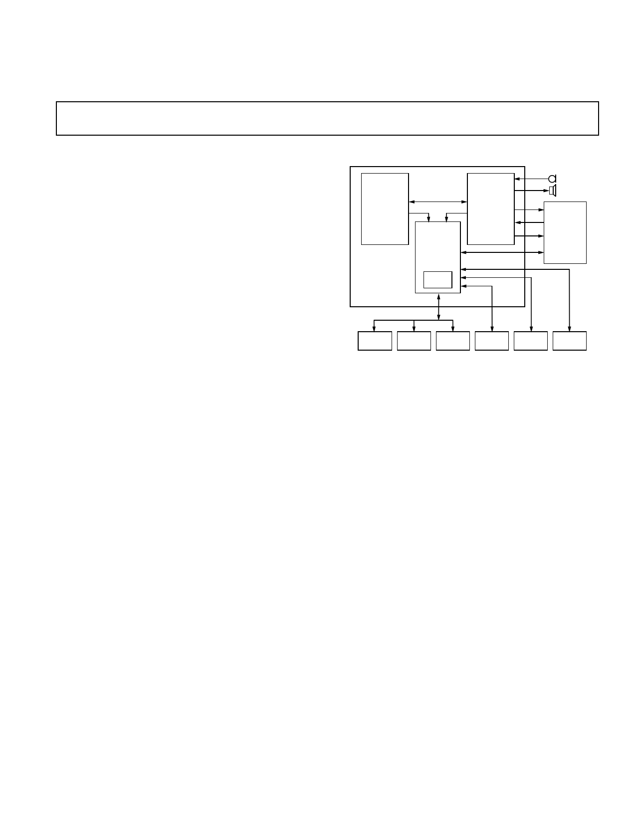
AD20msp410
SYSTEM ARCHITECTURE
ALGORITHM
SIGNAL
PROCESSOR
ASP
PHYSICAL
LAYER
PROCESSOR
AD20msp410
GSM CHIPSET
PLP
µC
BASEBAND
CONVERTER
BBC
RADIO
SUBSYSTEM
512K x 16 128K x 8
ROM
RAM
DISPLAY
2K x 8
EEPROM
KEYPAD
SIM
GENERAL DESCRIPTION
The Analog Devices GSM baseband processing chipset provides
a competitive solution for GSM based mobile radio systems. It
is designed to be fully integrated, easy to use, and compatible
with a wide range of product solutions. GSM phones using this
chipset and its accompanying Layer 1, 2, 3 software have passed
the European GSM full type approval process.
The chipset consists of three highly integrated, sub-micron, low
power CMOS components that form the core baseband signal
processing of the GSM handset. The system architecture is
designed to be easily integrated into current designs and form
the basis of next generation of designs.
The chipset uses an operating voltage of 2.7 V to 3.6 V, which
coupled with the extensive power management features,
significantly reduces the drain on battery power and extends the
handset’s talktime and standby time.
CHIPSET COMPONENTS
Algorithm Signal Processor (ASP)
The ASP is an application specific variant of the ADSP-2171
standard DSP from Analog Devices. It has been optimized to
meet the cost, size and power consumption requirements of
GSM mobile applications. All necessary memory to run the
GSM specific programs is provided on-chip and with its
preprogrammed ROM, no user programming is required. The
ASP implements full rate speech transcoding according to GSM
specifications, including Discontinuous Transmission (DTX)
and Comfort Noise Insertion (CNI). A high performance soft-
decision Viterbi equalizer is also implemented in software,
embedded in the ROM.
Physical Layer Processor (PLP)
The PLP combines application specific hardware and an
embedded 16-bit microcontroller (Hitachi H8/300H) to
perform channel coding and decoding and execute the protocol
stack and user software. The embedded processor executes the
Layer 1, 2, 3 and user MMI software. The PLP can control all
powerdown functions of the other chips and memory support
components to achieve maximum power savings.
Baseband Converter (BBC)
The BBC performs the voiceband and baseband analog-to-
digital and digital-to-analog conversions, interfacing the digital
sections of the chipset to the microphone, loudspeaker and radio
section. In addition, the BBC contains all the auxiliary convert-
ers for burst-ramping, AFC, AGC, battery and temperature
monitoring. The chipset interfaces directly with a variety of
industry standard radio architectures and supplies all the
synthesizer and timing control signals.
REV. 0
Information furnished by Analog Devices is believed to be accurate and
reliable. However, no responsibility is assumed by Analog Devices for its
use, nor for any infringements of patents or other rights of third parties
which may result from its use. No license is granted by implication or
otherwise under any patent or patent rights of Analog Devices.
© Analog Devices, Inc., 1996
One Technology Way, P.O. Box 9106, Norwood, MA 02062-9106, U.S.A.
Tel: 617/329-4700
Fax: 617/326-8703
1 page 
AD20msp410
• Full engineering and test mode support
• Support for all phase 1 and phase 2 handover modes
• SIM Interface driver
• Message interfacing to Layer 3 (Radio Resources Manager)
and Layer 2 (data link layer, both signaling and data)
• External functions for AGC, AFC and synthesizer setting are
called by Layer 1. These allow the user to configure the
system for a wide range of radio architectures including the
TTP GSM reference radio.
• The higher layers of the protocol stack also reside on this
embedded processor. A GSM Phase 2 compliant, Layer 2/3
protocol stack is available from The Technology Partnership.
POWER DISSIPATION CONSIDERATIONS
In mobile applications, minimizing the power consumption of
all devices is critical to achieving longer standby and talk times.
In a GSM handset the baseband subsystem dominates the
current consumption of the phone in standby. The design of the
ASP, PLP and BBC includes extensive features to reduce current
consumption and give standby times of up to 70 hours.
All three devices were specifically designed to operate from
2.7 V to 3.6 V, so facilitating three or four cell NiCad/NiMH or
single-cell Li Ion batteries.
The PLP incorporates intelligent power management, permit-
ting automatic control of power consumption in the PLP and
the peripheral circuitry. Data processing modules are switched
on only when they process data, otherwise they are powered
down.
Additional control signals are provided that enable the Layer 1
software to control the external subsystems, such as the ASP,
BBC, radio and memory components, so that their power is
intelligently switched by the PLP.
Within the ASP the different powerdown modes range from a
simple “wait for interrupt” state to a complete hardware
powerdown, with only leakage currents dissipating power.
In the BBC, the powerdown functions are split separately
between receive, transmit and auxiliary circuits. This provides
optimal analog power performance when operating in different
modes.
INTERFACES
Figure 5 shows the chipset’s eight interfaces, which have to be
considered in the design of the complete mobile radio. Some of
these interfaces have to meet GSM specifications, others will be
design specific.
• Analog Voice Interface to BBC
• Radio Interface to BBC and PLP
• Digital SIM Card Interface to PLP
• Digital Interface to the Keypad
• Digital Bus Interface from PLP to Memory and Display
• Digital Interface from the PLP to the EEPROM
• Digital Audio Interface (DAI)
• Digital Interface to PLP for Data Services
Analog Voice Interface to BBC
The analog voice interface to the BBC is specified in the
AD7015 data sheet. Several design examples are given for
single-ended or differential inputs or outputs. A voltage
reference for biasing the microphone signal is provided on the
BBC. The analog output of the BBC is capable of driving an
earpiece directly with and impedance of 150 Ω. For optional
use of a separate external microphone and power amplifier, a set
of auxiliary inputs/outputs is provided.
Radio Interface to BBC and PLP
The analog interface between the BBC and the radio subsystem
consists of differential inputs and outputs for the I and Q parts
of the signal and three analog control signals for AFC, AGC and
transmit ramp envelope. Details of these signals are specified in
the AD7015 data sheet. The digital interface between the PLP
and the radio subsystem consists of a serial port for communi-
cating with the synthesizers and several control signals as
specified in detail in the ADPLP01 data sheet.
Digital SIM Card Interface to PLP
The PLP is designed to interface directly to the SIM. However
interface logic may be necessary to connect the 3 V chipset to a
5 V SIM.
Digital Interface to Keypad
Keypad interface logic for up to 40 keys is provided on the PLP.
This interface provides keyboard scan for 8 Rows and 4
columns. Additionally an extra pin on the PLP is provided for
the power switch.
Digital Bus Interface to Memory and Display
External RAM and ROM as well as the display controller
interfaces directly to the 21-bit address bus and 16-bit data bus
of the PLP.
Interface to FLASH Memory
The large FLASH memory can contain all programs for the
embedded Control Processor of the PLP. This includes the
complete GSM protocol software as well as the User Interface
Software. A size of 4 Mbit to 8 Mbit is suggested to accommo-
date all Protocol software plus a typical size of User Interface
Software. Enhanced features, requiring larger memories are
supported easily by the large address space of the embedded
Control Processor. To facilitate production programming and
field upgrades of the FLASH memories, the PLP provides
embedded code to download the software into the FLASH
memory via its standard serial port.
Interface to SRAM
Beside the FLASH memory, the Control Processor additionally
supports static RAM to store user defined variables, typically
those used by the Protocol Stack or Application Layer. Standard
SRAMs interface directly to the address and data bus of the
PLP.
Interface to Display Controller
This interface is achieved through the address and data buses
and associated read and write strobes, as well as a specific
enable signal. An integrated wait state generator helps interface
to a wide range of display controllers. Two pins with PWM
outputs control the intensity of separate backlights for display
and keypad.
REV. 0
–5–
5 Page | ||
| Páginas | Total 8 Páginas | |
| PDF Descargar | [ Datasheet ADPLP01.PDF ] | |
Hoja de datos destacado
| Número de pieza | Descripción | Fabricantes |
| ADPLP01 | GSM Baseband Processing Chipset | Analog Devices |
| Número de pieza | Descripción | Fabricantes |
| SLA6805M | High Voltage 3 phase Motor Driver IC. |
Sanken |
| SDC1742 | 12- and 14-Bit Hybrid Synchro / Resolver-to-Digital Converters. |
Analog Devices |
|
DataSheet.es es una pagina web que funciona como un repositorio de manuales o hoja de datos de muchos de los productos más populares, |
| DataSheet.es | 2020 | Privacy Policy | Contacto | Buscar |