|
|
|
PDF ADP3421JRU Data sheet ( Hoja de datos )
| Número de pieza | ADP3421JRU | |
| Descripción | Geyserville-Enabled DC-DC Converter Controller for Mobile CPUs | |
| Fabricantes | Analog Devices | |
| Logotipo | ||
Hay una vista previa y un enlace de descarga de ADP3421JRU (archivo pdf) en la parte inferior de esta página. Total 12 Páginas | ||
|
No Preview Available !
a
Geyserville-Enabled DC-DC
Converter Controller for Mobile CPUs
FEATURES
Meets Intel® Mobile Voltage Positioning Requirements
Lowest Processor Dissipation for Longest Battery Life
Best Transient Containment
Minimum Number of Output Capacitors
System Power Management Compliant
Fast, Smooth Output Transition During VID Code
Change
Programmable Current Limit
Power Good
Integrated LDO Controllers for Clock and I/O Supplies
Programmable UVLO
Soft Start with Restart Lock-In
APPLICATIONS
Geyserville-Enabled Core DC-DC Converters
Fixed Voltage Mobile CPU Core DC-DC Converters
Notebook/Laptop Power Supplies
Programmable Output Power Supplies
GENERAL DESCRIPTION
The ADP3421 is a hysteretic dc-dc buck converter controller
with two auxiliary linear regulator controllers. The ADP3421
provides a total power conversion control solution for a micro-
processor by delivering the core, I/O, and clock voltages. The
optimized low-voltage design is powered from the 3.3 V system
supply and draws only 10 µA maximum in shutdown. The main
output voltage is set by a 5-bit VID code. To accommodate the
transition time required by the newest processors for on-the-
fly VID changes, the ADP3421 features high-speed operation
to allow a minimized inductor size that results in the fastest change
of current to the output. To further allow for the minimum
number of output capacitors to be used, the ADP3421 features
active voltage positioning that can be optimally compensated
to ensure a superior load transient response. The main output
signal interfaces with the ADP3410 dual MOSFET driver,
which is optimized for high speed and high efficiency for driving
both the upper and lower (synchronous) MOSFETs of the
buck converter.
DACOUT
VID4
VID3
VID2
VID1
VID0
LTO
LTB
LTI
CLKDRV
CLKFB
IODRV
IOFB
UVLO
VCC
GND
SD
ADP3421
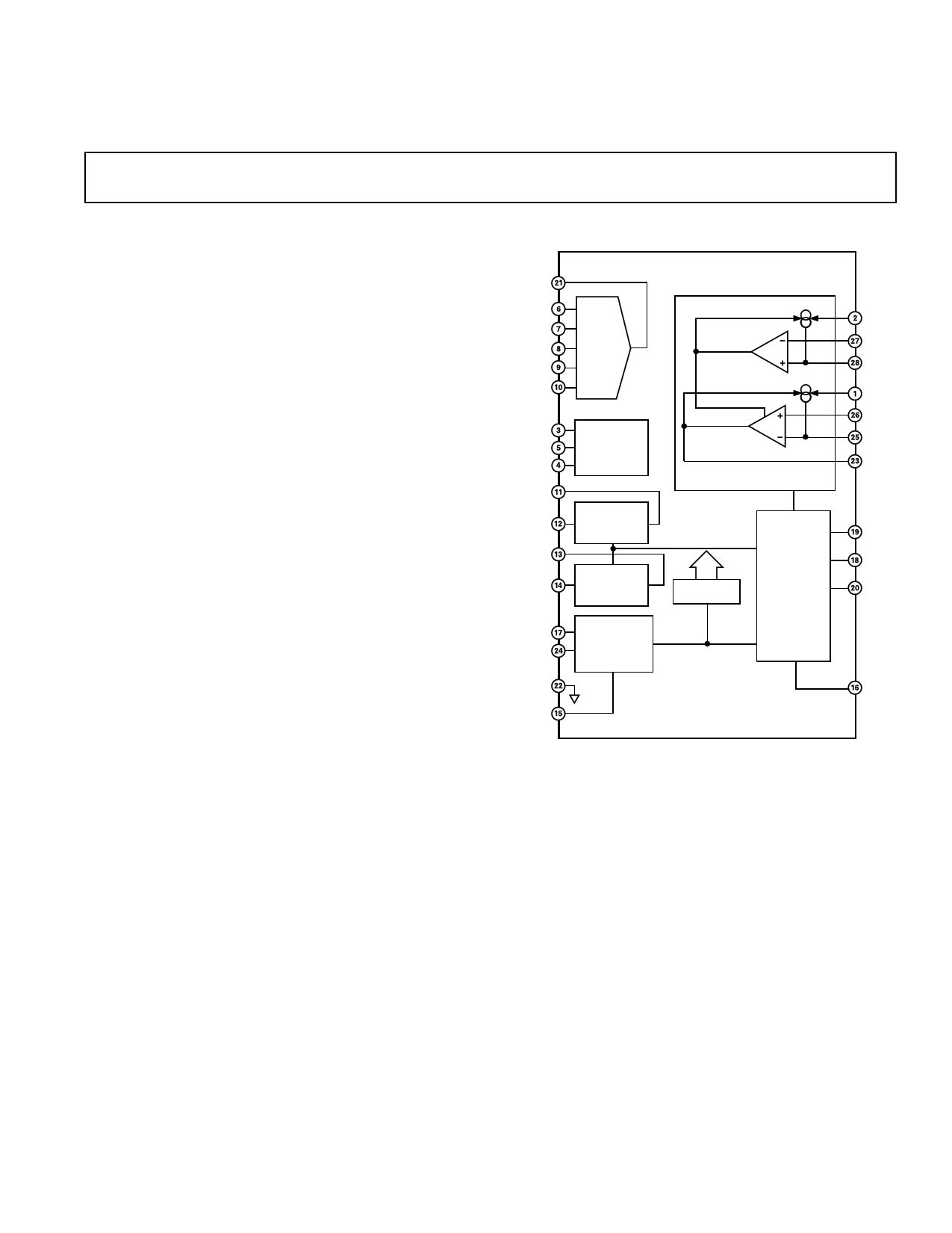
FUNCTIONAL BLOCK DIAGRAM
ADP3421
VID DAC
CURRENT
LIMIT
COMPARATOR
EN
LEVEL
TRANSLATOR
CORE
COMPARATOR
CORE CONTROLLER
CLOCK LDO
CONTROLLER
I/O LDO
CONTROLLER
VIN/VCC
MONITOR AND
UVLO BIAS
REFERENCE
CONTROLLER
BIAS AND
REFERENCE
BIAS EN
SOFT START
TIMER
AND
POWER GOOD
GENERATOR
CLSET
CS+
CS–
VHYS
REG
RAMP
OUT
SSC
SSL
CORE
PWRGD
REV. A
Information furnished by Analog Devices is believed to be accurate and
reliable. However, no responsibility is assumed by Analog Devices for its
use, nor for any infringements of patents or other rights of third parties that
may result from its use. No license is granted by implication or otherwise
under any patent or patent rights of Analog Devices.
One Technology Way, P.O. Box 9106, Norwood, MA 02062-9106, U.S.A.
Tel: 781/329-4700
www.analog.com
Fax: 781/326-8703
© Analog Devices, Inc., 2002
1 page 
ADP3421
Pin Mnemonic Function
15 SD
16 PWRGD
Shutdown Input. When this pin is pulled low, the IC shuts down and all regulation functions will be disabled.
Power Good Output. This signal will go high only when the SD pin is high to allow IC operation, the UVLO
and VCC pins are above their respective start-up thresholds, the SSC and SSL pins are above a voltage where
soft start is completed, and the voltage at the CORE pin is within the specified limits of the programmed VID
voltage. By choosing the soft-start capacitor for the core larger than that for the linear regulators, at start-up
the core and linear outputs should all be in regulation before PWRGD is asserted.
17 UVLO
Undervoltage Lockout Input. This pin monitors the input voltage through a resistor divider. When the pin
voltage is below a specified threshold, the IC enters into UVLO mode regardless of the status of SD. When
in UVLO mode, a current source is switched on at this pin, which sinks current from the external resistor
divider. The generated UVLO hysteresis is equal to the current sink value times the upper divider resistor.
18 SSL
Linear Regulator Soft Start. During power-up, an external soft-start capacitor is charged by a current source
to control the ramp-up rates of the linear regulators.
19 SSC
Core Voltage Soft Start. During power-up, an external soft-start capacitor is charged by a current source to
control the ramp-up rate of the core voltage.
20 CORE
Core Converter Voltage Monitor. This pin is used to monitor the core voltage for power good verification.
21 DACOUT VID-Programmed Digital-to-Analog Converter Output. This voltage is the reference voltage for output
voltage regulation.
22 GND
Ground
23 OUT
Logic-Level Drive Signal Output of Core Controller. This pin provides the drive command signal to the IN
pin of the ADP3410 driver. This pin is not capable of directly driving a power MOSFET.
24 VCC
25 RAMP
Power Supply
Current Ramp Input. This pin provides the negative feedback for the core output voltage. The switched sink/
source current from this pin, which is set up at the VHYS pin, works against the terminating resistance at this
pin to set the hysteresis for the hysteretic control.
26 REG
Regulation Voltage Summing Input. In the recommended configuration, the DACOUT voltage and the core
voltage are summed at this pin to establish regulation with output voltage positioning.
27 CS+
Current Limit Positive Sense. This pin senses the positive node of the current sense resistor.
28 CS–
Current Limit Negative Sense. This pin connects through a resistor to the negative node of the current sense
resistor. A current flows out of the pin, as programmed at the CLSET pin. When this pin is more negative
than the CS+ pin, the current limit comparator is triggered and the current flowing out of the pin is reduced
to two-thirds of its previous value, producing a current limit hysteresis.
REV. A
–5–
5 Page 
ADP3421
Power Switching Circuitry
ADP3410, MOSFETs, Input Capacitors
3. Locate the ADP3410 near the MOSFETs so the parasitic
inductance in the gate drive traces and the trace to the SW
pin is small, and so that the ground pins of the ADP3410
are closely connected to the lower MOSFET’s source.
4. Locate at least one substantial (i.e., > ~1 µF) input bypass
MLC capacitor close to the MOSFETs so that the physical
area of the loop enclosed in the electrical path through the
bypass capacitor and around through the top and bottom
MOSFETs (drain-source) is small. This is the switching
power path loop.
5. Make provisions for thermal management of all the MOSFETs.
Heavy copper and wide traces to ground and power planes will
help to pull out the heat. Heat sinking by a metal tap soldered
in the power plane near the MOSFETs will help. Even just
small airflow can help tremendously. Paralleled MOSFETs will
help spread the heat, even if the on resistance is higher.
6. An external “antiparallel” Schottky diode (across the bottom
MOSFET) may help efficiency a small amount (< ~1 %); a
MOSFET with a built-in antiparallel Schottky is more
effective. For an external Schottky, it should be placed next
to the bottom MOSFET or it may not be effective at all.
Also, a higher current rating (bigger device with lower voltage
drop) is more effective.
7. Both ground pins of the ADP3410 should be connected into
the same ground plane with the power switching circuitry,
and the VCC bypass capacitor should be close to the VCC
pin and connected into the same ground plane.
Output Filter
Output Inductor and Capacitors, Current-Sense Resistor
8. Locate the current-sense resistor very near to the output
capacitors.
9. PCB trace resistances from the current-sense resistor to the
output capacitors, and from the output capacitors to the
load, should be minimized, known (calculated or measured),
and compensated for as part of the design if it is significant.
(Remote sensing is not sufficient for relieving this require-
ment.) A square section of 1 ounce copper trace has a
resistance of ~500 mΩ. Using 2~3 squares of copper can
make a noticeable impact on a 15 A design.
10. Whenever high currents must be routed between PCB layers,
vias should be used liberally to create several parallel current
paths so that the resistance and inductance introduced by
these current paths is minimized and the via current rating
is not exceeded.
11. The ground connection of the output capacitors should be
close to the ground connection of the lower MOSFET and
it should be a ground plane. Current may pulsate in this
path if the power source ground is closer to the output
capacitors than the power switching circuitry, so a close
connection will minimize the voltage drop.
Control Circuitry
ADP3421, Control Components
12. If the placement overview cannot be followed, the ground
pin of the ADP3421 should be Kelvin-connected into the
ground plane near the output capacitors to avoid introduc-
ing ground noise from the power switching stage into the
control circuitry. All other control components should be
grounded on that same signal ground.
13. If critical signal lines (i.e., signals from the current-sense
resistor leading back to the ADP3421) must cross through
power circuitry, it is best if a signal ground plane can be
interposed between those signal lines and the traces of the
power circuitry. This serves as a shield to minimize noise
injection into the signals at the expense of making signal
ground a bit noisier.
14. Absolutely avoid crossing any signal lines over the switching
power path loop, as previously described.
15. Accurate voltage positioning depends on accurate current
sensing, so the control signals that differentially monitor
the voltage across the current-sense resistor should be
Kelvin-connected.
16. The RC filter used for the current-sense signal should be
located near the control components.
LDOs
PNP Transistors
17. The maximum steady-state power dissipation expected
for the design should be calculated so that an acceptable
package type PNP for each output is selected and properly
mounted to be able to dissipate the power with acceptable
temperature rise.
18. Each PNP transistor should be located close to the load that
it sources.
19. The supply voltage to the PNP emitters should be low
impedance to avoid loop instability. It is good design practice
to have at least one MLC capacitor near each of the PNP
emitters to help ensure the impedance is sufficiently low.
REV. A
–11–
11 Page | ||
| Páginas | Total 12 Páginas | |
| PDF Descargar | [ Datasheet ADP3421JRU.PDF ] | |
Hoja de datos destacado
| Número de pieza | Descripción | Fabricantes |
| ADP3421JRU | Geyserville-Enabled DC-DC Converter Controller for Mobile CPUs | Analog Devices |
| Número de pieza | Descripción | Fabricantes |
| SLA6805M | High Voltage 3 phase Motor Driver IC. |
Sanken |
| SDC1742 | 12- and 14-Bit Hybrid Synchro / Resolver-to-Digital Converters. |
Analog Devices |
|
DataSheet.es es una pagina web que funciona como un repositorio de manuales o hoja de datos de muchos de los productos más populares, |
| DataSheet.es | 2020 | Privacy Policy | Contacto | Buscar |