|
|
|
PDF ADP3335 Data sheet ( Hoja de datos )
| Número de pieza | ADP3335 | |
| Descripción | High Accuracy Ultralow IQ/ 500 mA anyCAP Low Dropout Regulator | |
| Fabricantes | Analog Devices | |
| Logotipo | ||
Hay una vista previa y un enlace de descarga de ADP3335 (archivo pdf) en la parte inferior de esta página. Total 8 Páginas | ||
|
No Preview Available !
a
High Accuracy Ultralow IQ, 500 mA
anyCAP® Low Dropout Regulator
ADP3335
FEATURES
High Accuracy Over Line and Load: ؎0.9% @ 25؇C,
؎1.8% Over Temperature
Ultralow Dropout Voltage: 200 mV (Typ) @ 500 mA
Requires Only CO = 1.0 F for Stability
anyCAP = Stable with Any Type of Capacitor
(Including MLCC)
Current and Thermal Limiting
Low Noise
Low Shutdown Current: < 1.0 A
2.6 V to 12 V Supply Range
–40؇C to +85؇C Ambient Temperature Range
Ultrasmall Thermally-Enhanced 8-Lead MSOP Package
APPLICATIONS
PCMCIA Card
Cellular Phones
Camcorders, Cameras
Networking Systems, DSL/Cable Modems
Cable Set-Top Box
MP3/CD Players
DSP Supply
GENERAL DESCRIPTION
The ADP3335 is a member of the ADP330x family of precision
low dropout anyCAP voltage regulators. The ADP3335 operates
with an input voltage range of 2.6 V to 12 V and delivers a con-
tinuous load current up to 500 mA. The ADP3335 stands out
from conventional LDOs with the lowest thermal resistance of
any MSOP-8 package and an enhanced process that enables it
to offer performance advantages beyond its competition. Its
patented design requires only a 1.0 µF output capacitor for sta-
bility. This device is insensitive to output capacitor Equivalent
Series Resistance (ESR), and is stable with any good quality
capacitor, including ceramic (MLCC) types for space-restricted
applications. The ADP3335 achieves exceptional accuracy of
± 0.9% at room temperature and ± 1.8% over temperature, line,
and load. The dropout voltage of the ADP3335 is only 200 mV
(typical) at 500 mA. This device also includes a safety current
limit, thermal overload protection and a shutdown feature. In
shutdown mode, the ground current is reduced to less than
1 µA. The ADP3335 has ultralow quiescent current 80 µA
(typical) in light load situations.
IN
SD
FUNCTIONAL BLOCK DIAGRAM
THERMAL
PROTECTION
Q1
CC
DRIVER
ADP3335
gm
BANDGAP
REF
OUT
R1
NR
R2
GND
VIN
C IN
1F
+
NR
ADP3335
OUT
IN OUT
IN OUT
SD GND
ON
OFF
VOUT
+ COUT
1F
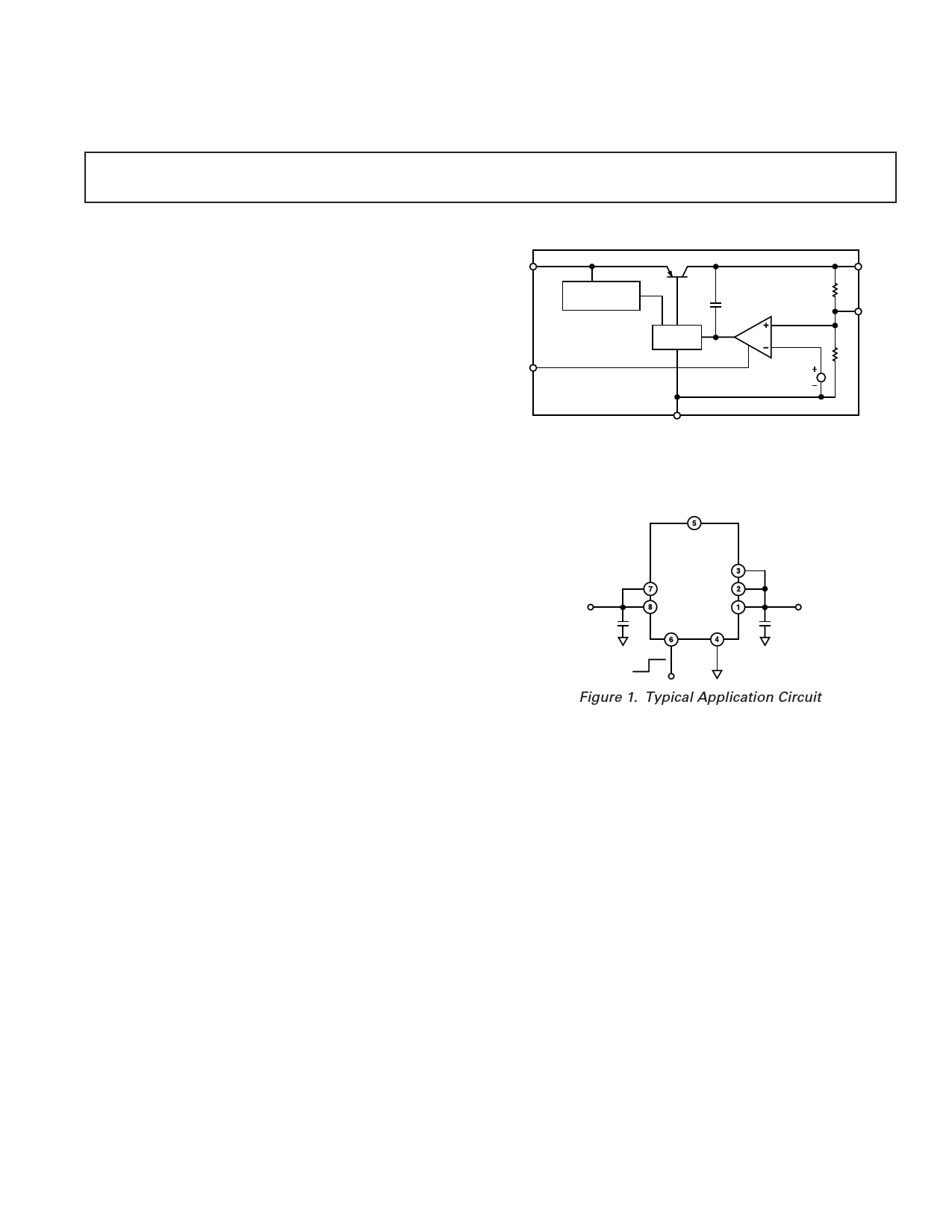
Figure 1. Typical Application Circuit
anyCAP is a registered trademark of Analog Devices Inc.
REV. 0
Information furnished by Analog Devices is believed to be accurate and
reliable. However, no responsibility is assumed by Analog Devices for its
use, nor for any infringements of patents or other rights of third parties
which may result from its use. No license is granted by implication or
otherwise under any patent or patent rights of Analog Devices.
One Technology Way, P.O. Box 9106, Norwood, MA 02062-9106, U.S.A.
Tel: 781/329-4700 World Wide Web Site: http://www.analog.com
Fax: 781/326-8703
© Analog Devices, Inc., 2000
1 page 
ADP3335
2.210
2.200
2.190
2.189
2.179
3.500
3.000
VOUT = 2.2V
RL = 4.4⍀
CL = 1F
40 80 140 180
TIME – s
2.210
2.200
2.190
2.189
2.179
3.500
3.000
VOUT = 2.2V
RL = 4.4⍀
CL = 10F
40 80 140 180
TIME – s
2.3
2.2
2.1
VIN = 4V
VOUT = 2.2⍀
CL = 1F
400
200
0
200 400
600
TIME – s
800
Figure 11. Line Transient Response
Figure 12. Line Transient Response
Figure 13. Load Transient Response
2.3
2.2
2.1
VOUT = 2.2V
RL = 4.4⍀
CL = 10F
400
200
0
200 400 600 800
TIME – s
2.2
0
FULL SHORT
3 800m⍀
SHORT
2
1 VIN = 4V
0
200 400
600
TIME – s
800
3 1F
2
1
0
10F
VIN = 6V
VOUT = 2.2V
RL = 4.4⍀
10F
1F
2
0
200 400 600 800
TIME – s
Figure 14. Load Transient Response
Figure 15. Short Circuit Current
Figure 16. Turn On–Turn Off Response
–20
VOUT = 2.2V
–30
CL = 1F
–40 IL = 500mA
CL = 10F
IL = 500mA
–50
CL = 1F
IL = 50A
–60
–70
–80
CL = 10F
IL = 50A
–90
10 100 1k 10k 100k 1M 10M
FREQUENCY – Hz
Figure 17. Power Supply Ripple
Rejection
160
CNR = 10nF
140
120
100
80
60
40
IL = 500mA WITHOUT
NOISE REDUCTION
IL = 500mA WITH
NOISE REDUCTION
IL = 0mA WITHOUT
NOISE REDUCTION
20
IL = 0mA WITH NOISE REDUCTION
0
0 10 20 30
CL – F
40
Figure 18. RMS Noise vs. CL
(10 Hz–100 kHz)
50
100
VOUT = 2.2V
IL = 1mA
10 CL = 10F CL = 10F
CNR = 10nF CNR = 0
CL = 1F
1 CNR = 0
0.1
0.01
CL = 1F
CNR = 10nF
0.001
10
100 1k 10k 100k
FREQUENCY – Hz
1M
Figure 19. Output Noise Density
REV. 0
–5–
5 Page | ||
| Páginas | Total 8 Páginas | |
| PDF Descargar | [ Datasheet ADP3335.PDF ] | |
Hoja de datos destacado
| Número de pieza | Descripción | Fabricantes |
| ADP3330 | Low Dropout Regulator | Analog Devices |
| ADP3331 | Adjustable Output Ultralow IQ/ 200 mA/ SOT-23/ anyCAP Low Dropout Regulator | Analog Devices |
| ADP3333 | High Accuracy Ultralow IQ/ 300 mA/ anyCAP Low Dropout Regulator | Analog Devices |
| ADP3334 | High Accuracy Low IQ/ 500 mA anyCAP Adjustable Low Dropout Regulator | Analog Devices |
| Número de pieza | Descripción | Fabricantes |
| SLA6805M | High Voltage 3 phase Motor Driver IC. |
Sanken |
| SDC1742 | 12- and 14-Bit Hybrid Synchro / Resolver-to-Digital Converters. |
Analog Devices |
|
DataSheet.es es una pagina web que funciona como un repositorio de manuales o hoja de datos de muchos de los productos más populares, |
| DataSheet.es | 2020 | Privacy Policy | Contacto | Buscar |