|
|
|
PDF ADP3170JRU Data sheet ( Hoja de datos )
| Número de pieza | ADP3170JRU | |
| Descripción | VRM 8.5 Compatible Single Phase Core Controller | |
| Fabricantes | Analog Devices | |
| Logotipo | ||
Hay una vista previa y un enlace de descarga de ADP3170JRU (archivo pdf) en la parte inferior de esta página. Total 16 Páginas | ||
|
No Preview Available !
a
FEATURES
Optimally Compensated Active Voltage Positioning
with Gain and Offset Adjustment (ADOPT™) for
Superior Load Transient Response
Complies with VRM 8.5 Specifications with Lowest
System Cost
5-Bit Digitally Programmable 1.05 V to 1.825 V Output
N-Channel Synchronous Buck Controller
Onboard 1.8 V Linear Regulator Controller
Total Accuracy ؎1% Over Temperature
High Efficiency Current-Mode Operation
Short Circuit Protection
Power Good Output
Overvoltage Protection Crowbar Protects
Microprocessors with No Additional External
Components
APPLICATIONS
Core and 1.8 V Standby Supplies for Next Generation
Intel Pentium® III Processors
VRM 8.5 Compatible
Single Phase Core Controller
ADP3170
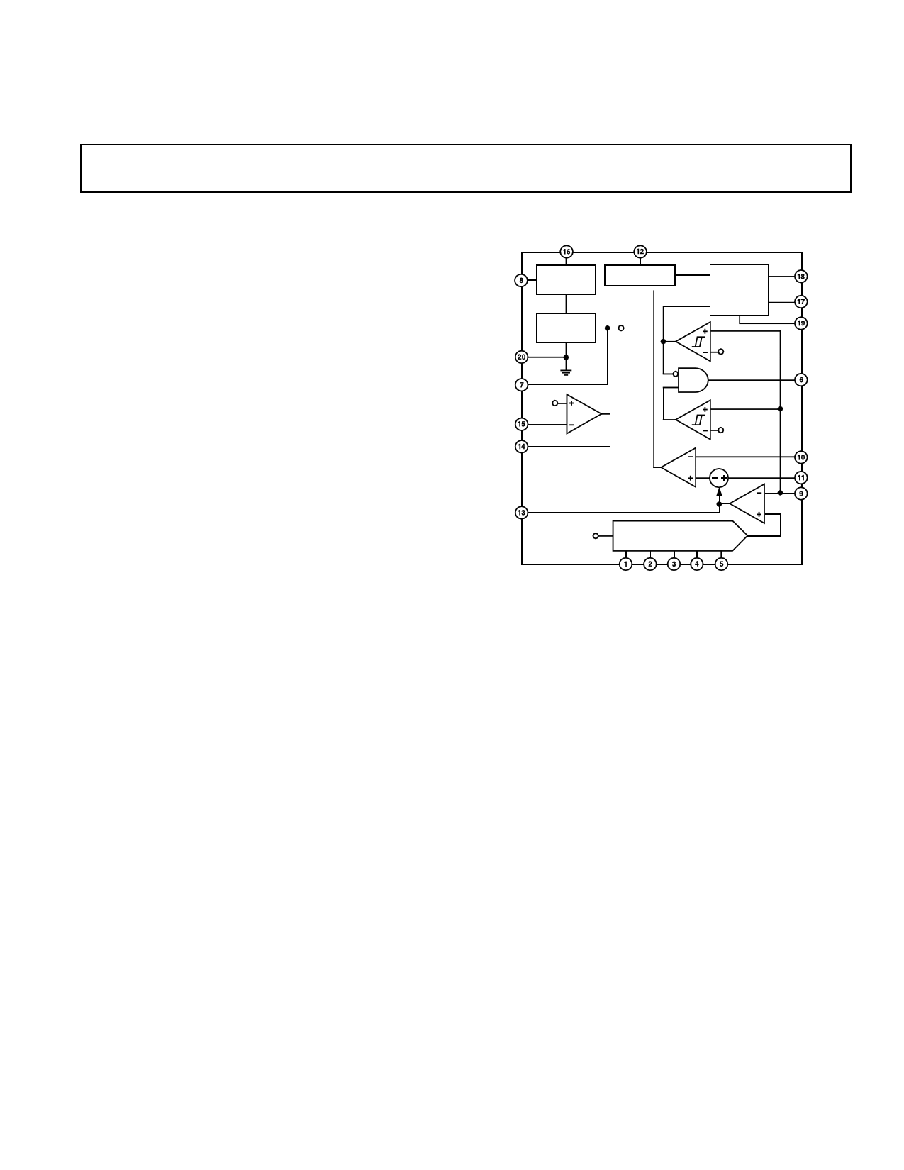
FUNCTIONAL BLOCK DIAGRAM
VCC
CT
SD
GND
UVLO
AND BIAS
3.0V
REFERENCE
OSCILLATOR
SET
RESET
CROWBAR
PWM
LOGIC
REF
DAC +20%
REF
LRFB
LRDRV
1.8V
COMP
ADP3170
REF
CMP
VID
DAC
DAC –20%
gm
DRVH
DRVL
PGND
PWRGD
CS–
CS+
FB
VID3 VID2 VID1 VID0 VID25
GENERAL DESCRIPTION
The ADP3170 is a highly efficient output synchronous buck
switching regulator controller optimized for converting a 5 V
main supply into the core supply voltage required by next
generation Intel Celeron processors. The ADP3170 uses an
internal 5-bit DAC to read a voltage identification (VID)
code directly from the processor, which is used to set the
output voltage between 1.05 V and 1.825 V. The ADP3170
uses a current mode, constant off-time architecture to drive two
N-channel MOSFETs at a programmable switching frequency
that can be optimized for regulator size and efficiency.
The ADP3170 also uses a unique supplemental regulation tech-
nique called Analog Devices Optimal Positioning Technology
(ADOPT) to enhance load transient performance. Active
voltage positioning results in a dc/dc converter that meets the
stringent output voltage specifications for high performance
processors, with the minimum number of output capacitors and
smallest footprint. Unlike voltage-mode and standard current-
mode architectures, active voltage positioning adjusts the output
voltage as a function of the load current so that it is always
optimally positioned for a system transient. The ADP3170 also
provides accurate and reliable short circuit protection and
adjustable current limiting. It also includes an integrated
overvoltage crowbar function to protect the microprocessor
from destruction in case the core supply exceeds the nominal
programmed voltage by more than 20%.
The ADP3170 contains a 1.8 V linear regulator controller that
is designed to drive an external N-channel MOSFET. This linear
regulator can be used to generate auxiliary voltages (such as 1.8 V
standby power) required in most motherboard designs, and has
been designed to provide a high bandwidth load-transient response.
The ADP3170 is specified over the commercial temperature range
of 0°C to 70°C and is available in a 20-lead TSSOP package.
ADOPT is a trademark of Analog Devices, Inc.
Pentium is a registered trademark of Intel Corporation
REV. 0
Information furnished by Analog Devices is believed to be accurate and
reliable. However, no responsibility is assumed by Analog Devices for its
use, nor for any infringements of patents or other rights of third parties that
may result from its use. No license is granted by implication or otherwise
under any patent or patent rights of Analog Devices.
One Technology Way, P.O. Box 9106, Norwood, MA 02062-9106, U.S.A.
Tel: 781/329-4700
www.analog.com
Fax: 781/326-8703
© Analog Devices, Inc., 2001
1 page 
5-BIT CODE
VFB
ADP3170
1 VID3
2 VID2
3 VID1
4 VID0
5 VID25
6 PWRGD
7 REF
8 SD
9 FB
10 CS–
GND 20
PGND 19
DRVH 18
DRVL 17
VCC 16
LRFB 15
LRDRV 14
COMP 13
CT 12
CS+ 11
12V
1F 100nF
100⍀
100nF
AD820
1.2V
Figure 1. Closed-Loop Output Voltage Accuracy
Test Circuit
ADP3170
ADP3170
1 VID3
2 VID2
3 VID1
4 VID0
5 VID25
6 PWRGD
7 REF
8 SD
9 FB
10 CS–
GND 20
PGND 19
DRVH 18
DRVL 17
VCC 16
LRFB 15
LRDRV 14
COMP 13
CT 12
CS+ 11
VCC
1F 100nF
VLR
10nF
Figure 2. Linear Regulator Output Voltage Accuracy
Test Circuit
REV. 0
–5–
5 Page 
ADP3170
1
RA = 1 1 1
––
RT ROGM RB
RA = 1
1
1
1 = 12.83 kΩ
8.88 kΩ – 1 MΩ – 29.7 kΩ
(13)
Choosing the nearest 1% resistor value gives RA = 12.7 kΩ.
COUT Selection
The required equivalent series resistance (ESR) and capacitance
drive the selection of the type and quantity of the output capaci-
tors. The ESR of the output filter capacitor bank must be equal
to or less than the specified output resistance of the voltage
regulator (3.2 mΩ). The capacitance must be large enough that
the voltage across the capacitor, which is the sum of the resistive
and capacitive voltage drops, does not move below or above the
initial resistive step while the inductor current ramps up or
down to the value corresponding to the new load current. One
can use, for example, eight ZA series capacitors from Rubycon,
which have a maximum ESR of 24 mΩ. These eight 1000 µF
capacitors would give an ESR of 3 mΩ.
As long as the capacitance of the output capacitor is above a
critical value, and the regulating loop is compensated with
Analog Devices’ proprietary compensation technique (ADOPT),
the actual value has no influence on the peak-to-peak deviation
of the output voltage to a full step change in the load current.
The critical capacitance can be calculated as follows:
COUT (CRIT )
=
ROUT
IO
× (VOUT
+V –) × L
(14)
23A
COUT(CRIT ) = 3.2 mΩ × (1.8V + [–29 mV ]) × 1 µH = 4.06 mF
The equivalent capacitance of the eight ZA series Rubycon
capacitors is 8 × 1 mF = 8 mF. In this case, the total capacitance
is safely above the critical value.
Feedback Loop Compensation Design for ADOPT
Optimized compensation of the ADP3170 allows the best pos-
sible containment of the peak-to-peak output voltage deviation.
The output current slew rate of any practical switching power
converter is inherently limited by the inductor to a value much
less than the slew rate of the load. Therefore, any sudden change
of load current will initially flow through the output capacitors,
and assuming that the capacitance of the output capacitor is
larger than the critical value defined by Equation 14, this will
produce a peak output voltage deviation equal to the ESR of the
output capacitor times the load current change.
The optimal implementation of voltage positioning, ADOPT,
will create an output impedance of the power converter that is
entirely resistive over the widest possible frequency range,
including dc, and equal to the specified dc output resistance.
With the wide-band resistive output impedance the output
voltage will droop in proportion with the load current at any
load current slew rate; this ensures the optimal positioning
and allows the minimization of the output capacitor.
With an ideal current-mode controlled converter, where the
inductor current would respond without delay to the command
signal, the resistive output impedance could be achieved by
having a single-pole roll-off of the voltage gain of the voltage-
error amplifier. The pole frequency must coincide with the ESR
zero of the output capacitor.
The ADP3170 uses peak-current control, which is known to
have a nonideal, frequency-dependent command signal-to-
inductor current transfer function. The frequency dependence
manifests in the form of a pair of complex conjugate poles at
one-half of the switching frequency. A purely resistive output
impedance could be achieved by canceling the complex conju-
gate with zeros at the same complex frequencies and adding a
third pole equal to the ESR zero of the output capacitor. Such a
compensating network would be quite complicated. Fortu-
nately, in practice, it is sufficient to cancel the pair of complex
conjugate poles with a single real zero placed at one-half of the
switching frequency.
Although the end result is not a perfectly resistive output imped-
ance, the remaining frequency dependence causes only a slight
percentage of deviation from the ideal resistive response. The
single-pole and single-zero compensation can be easily imple-
mented by terminating the gm error amplifier with the parallel
combination of a resistor (RT) and a series RC network. The
value of the terminating resistor RT was determined previously;
the capacitance and resistance of the series RC network are
calculated as follows:
COC
=
COUT ×
RT
ESR
COC
=
8 mF × 3 mΩ
8.88 kΩ
=
2.7 nF
(15)
The closest standard value is 2.7 nF. The series resistance is:
2
RZ = COC × π × fMIN
RZ
=
2.7
nF
×
2
π × 188
kHz
= 1255 Ω
(16)
The nearest standard 5% resistor value is 1.2 kΩ. Note that this
resistor is only required when COUT approaches CCRIT (within
25% or less). In this example, COUT >> CCRIT, and RZ can
therefore be omitted.
REV. 0
–11–
11 Page | ||
| Páginas | Total 16 Páginas | |
| PDF Descargar | [ Datasheet ADP3170JRU.PDF ] | |
Hoja de datos destacado
| Número de pieza | Descripción | Fabricantes |
| ADP3170JRU | VRM 8.5 Compatible Single Phase Core Controller | Analog Devices |
| Número de pieza | Descripción | Fabricantes |
| SLA6805M | High Voltage 3 phase Motor Driver IC. |
Sanken |
| SDC1742 | 12- and 14-Bit Hybrid Synchro / Resolver-to-Digital Converters. |
Analog Devices |
|
DataSheet.es es una pagina web que funciona como un repositorio de manuales o hoja de datos de muchos de los productos más populares, |
| DataSheet.es | 2020 | Privacy Policy | Contacto | Buscar |