|
|
|
PDF ADM9240 Data sheet ( Hoja de datos )
| Número de pieza | ADM9240 | |
| Descripción | Low Cost Microprocessor System Hardware Monitor | |
| Fabricantes | Analog Devices | |
| Logotipo | ||
Hay una vista previa y un enlace de descarga de ADM9240 (archivo pdf) en la parte inferior de esta página. Total 22 Páginas | ||
|
No Preview Available !
a
Low Cost Microprocessor
System Hardware Monitor
ADM9240
FEATURES
Six Direct Voltage Measurement Inputs (IncludingTwo
Processor Core Voltages) with On-Chip Attenuators
On-Chip Temperature Sensor
Five Digital Inputs for VID Bits
Fully Supports Intel’s LANDesk Client Manager (LDCM)
Register-Compatible with LM7x Products
Two Fan Speed Monitoring Inputs
I2C® Compatible System Management Bus (SMBus)
Chassis Intrusion Detect
Interrupt Output
Programmable RESET I/O Pin
Shutdown Mode to Minimize Power Consumption
Limit Comparison of all Monitored Values
APPLICATIONS
Network Servers and Personal Computers
Microprocessor-Based Office Equipment
Test Equipment and Measuring Instruments
PRODUCT DESCRIPTION
The ADM9240 is a complete system hardware monitor for
microprocessor-based systems, providing measurement and
limit comparison of up to four power supplies and two proces-
sor core voltages, plus temperature, two fan speeds and chassis
intrusion. Measured values can be read out via an I2C-compat-
ible serial System Management Bus, and values for limit com-
parisons can be programmed in over the same serial bus. The
high speed successive approximation ADC allows frequent
sampling of all analog channels to ensure a fast interrupt
response to any out-of-limit measurement.
The ADM9240’s 2.85 V to 5.75 V supply voltage range, low
supply current and I2C compatible interface, make it ideal for a
wide range of applications. These include hardware monitoring
and protection applications in personal computers, electronic
test equipment and office electronics.
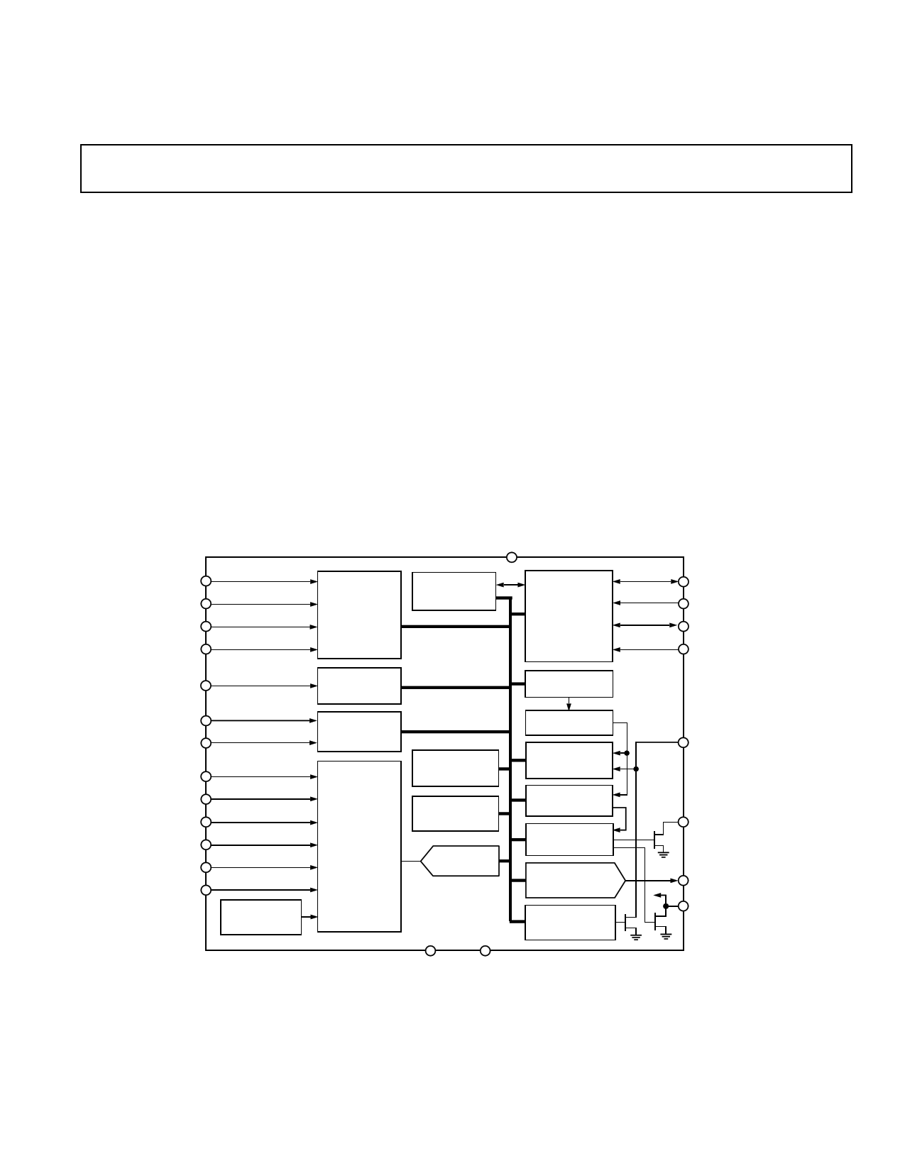
FUNCTIONAL BLOCK DIAGRAM
VCC
VID0
VID1
VID2
VID3
VID4
FAN1
FAN2
+VCCP1
+2.5VIN
+3.3VIN
+5VIN
+12VIN
+VCCP2
BANDGAP
TEMPERATURE
SENSOR
VID0 - 3 AND
FAN DIVISOR
REGISTERS
SERIAL BUS
ADDRESS
REGISTER
VID4 AND
DEVICE ID
REGISTER
FAN SPEED
COUNTER
INPUT
ATTENUATORS
AND
ANALOG
MULTIPLEXER
ADDRESS
POINTER
REGISTER
TEMPERATURE
CONFIGURATION
REGISTER
9-BIT ADC
ADM9240
GNDA
GNDD
SERIAL BUS
INTERFACE
VALUE AND LIMIT
REGISTERS
LIMIT
COMPARATORS
INTERRUPT
STATUS
REGISTERS
INT MASK
REGISTERS
CONFIGURATION
REGISTER
ANALOG
OUTPUT REGISTER
AND 8-BIT DAC
CHASSIS
INTRUSION
CLEAR REGISTER
NTEST_OUT/A0
A1
SDA
SCL
CI
INT
NTEST_IN/AOUT
RESET
I2C is a registered trademark of Philips Corporation.
REV. 0
Information furnished by Analog Devices is believed to be accurate and
reliable. However, no responsibility is assumed by Analog Devices for its
use, nor for any infringements of patents or other rights of third parties
which may result from its use. No license is granted by implication or
otherwise under any patent or patent rights of Analog Devices.
One Technology Way, P.O. Box 9106, Norwood, MA 02062-9106, U.S.A.
Tel: 781/329-4700 World Wide Web Site: http://www.analog.com
Fax: 781/326-8703
© Analog Devices, Inc., 1998
1 page 
ADM9240
PIN FUNCTION DESCRIPTIONS
Pin Number
1
2
3
4
5
6
7
8
9
10
11
12
13
14
15
16
17
18
19
20
21
22
23
24
Mnemonic
NTEST_OUT/A0
A1
SDA
SCL
FAN1
FAN2
CI
GNDD
VCC
INT
NTEST_IN/AOUT
RESET
GNDA
+VCCP2
+12 VIN
+5 VIN
+3.3 VIN
+2.5 VIN
+VCCP1
VID4
VID3
VID2
VID1
VID0
Description
Digital I/O. Dual Function Pin. The lowest order programmable bit of the Serial Bus Address.
This pin functions as an output when doing a NAND Tree test.
Digital Input. The highest order programmable bit of the Serial Bus Address.
Digital I/O. Serial Bus Bidirectional Data. Open-drain output.
Digital Input. Serial Bus Clock.
Digital Input. 0 to VCC amplitude fan tachometer input.
Digital Input. 0 to VCC amplitude fan tachometer input.
Digital I/O. An active high input from an external circuit that latches a Chassis Intrusion
event. This line can go high without any clamping action regardless of the powered state of
the ADM9240. The ADM9240 provides an internal open drain on this line, controlled by
Bit 6 of Register 40h or Bit 7 of Register 46h, to provide a minimum 20 ms pulse on this line,
to reset the external Chassis Intrusion Latch.
Digital Ground. Internally connected to all of the digital circuitry.
Power (+2.85 V to +5.75 V). Typically powered from +3.3 V or +5 V power rail. Bypass with
the parallel combination of 10 µF (electrolytic or tantalum) and 0.1 µF (ceramic) bypass
capacitors.
Digital Output. Interrupt Request (open drain). The output is enabled when Bit 1 of the
Configuration Register is set to 1. The default state is disabled.
Digital Input/Analog Output. An active-high input that enables NAND Tree mode board-
level connectivity testing. Refer to section on NAND Tree testing. Also functions as a pro-
grammable analog output when NAND Tree is not selected
Digital I/O. Master Reset, 5 mA driver (open drain), active low output with a 20 ms minimum
pulsewidth. Available when enabled via Bit 7 in Register 44h, and set using Bit 4 in Register
40h. Also acts as reset input when pulled low (e.g., power-on reset).
Analog Ground. Internally connected to all analog circuitry. The ground reference for all
analog inputs.
Analog Input. Monitors processor core voltage +VCCP2 (0 V–3.6 V). Can also be used to
monitor the –12 V supply by adding two external resistors.
Analog Input. Monitors +12 V supply.
Analog Input. Monitors +5 V supply.
Analog Input. Monitors +3.3 V supply.
Analog Input. Monitors +2.5 V supply.
Analog Input. Monitors processor core voltage +VCCP1 (0 V–3.6 V).
Digital Input. Core Voltage ID readouts from the processor. This value is read into the
VID4 Status Register.
Digital Input. Core Voltage ID readouts from the processor. This value is read into the
VID0–VID3 Status Register.
Digital Input. Core Voltage ID readouts from the processor. This value is read into the
VID0–VID3 Status Register.
Digital Input. Core Voltage ID readouts from the processor. This value is read into the
VID0–VID3 Status Register.
Digital Input. Core Voltage ID readouts from the processor. This value is read into the
VID0–VID3 Status Register.
REV. 0
–5–
5 Page 
ADM9240
MONITORING CYCLE TIME
The monitoring cycle begins when a one is written to the Start
Bit (Bit 0), and a zero to the INT_Clear Bit (Bit 3) of the Con-
figuration Register. INT_Enable (Bit 1) should be set to one to
enable the INT output. The ADC measures each analog input
in turn, starting with VCCP2 and finishing with the on-chip tem-
perature sensor. As each measurement is completed the result
is automatically stored in the appropriate value register. This
“round-robin” monitoring cycle continues until it is disabled by
writing a 0 to Bit 0 of the Configuration Register.
The counter controlling the multiplexer is driven by an on-chip
clock of nominally 22.5 kHz, so the entire measurement sequence
takes (nominally):
44.4 µs × 7 = 310.8 µs
This rapid sampling of the analog inputs ensures a quick re-
sponse in the event of any input going out of limits, unlike other
monitoring chips that employ slower ADCs.
When a monitoring cycle is started, monitoring of the fan speed
inputs begins at the same time as monitoring of the analog in-
puts. However, the two monitoring cycles are not synchronized
in any way, and the monitoring cycle time for the fan inputs is
dependent on fan speed and much slower than for the analog
inputs. For more details see the Fan Speed Measurement section.
INPUT SAFETY
Scaling of the analog inputs is performed on-chip, so external
attenuators are normally not required. However, since the
power supply voltages will appear directly at the pins, it is advis-
able to add small external resistors in series with the supply
traces to the chip to prevent damaging the traces or power sup-
plies should an accidental short such as a probe connect two
power supplies together.
As the resistors will form part of the input attenuators, they will
affect the accuracy of the analog measurement if their value is
too high. The analog input channels are calibrated assuming an
external series resistor of 500 Ω, and the accuracy will remain
within specification for any value from zero to 1 kΩ, so a stan-
dard 510 Ω resistor is suitable.
The worst such accident would be connecting –12 V to +12 V—
a total of 24 V difference, with the series resistors this would
draw a maximum current of approximately 24 mA.
ANALOG OUTPUT
The ADM9240 has a single analog output from an unsigned
8-bit DAC which produces 0 V–1.25 V. The analog output
register defaults to FF during power-on reset, which produces
maximum fan speed. The analog output may be amplified and
buffered with external circuitry such as an op amp and transistor
to provide fan speed control.
A suitable drive circuit is given in Figure 5.
Care must be taken when choosing the op amp to ensure that its
input common-mode range and output voltage swing are suitable.
The op amp may be powered from the +12 V rail alone or from
± 12 V. If it is powered from +12 V then the input common-
mode range should include ground to accommodate the mini-
mum output voltage of the DAC, and the output voltage should
swing below 0.6 V to ensure that the transistor can be turned
fully off.
If the op amp is powered from –12 V, precautions such as a
clamp diode to ground may be needed to prevent the base-
emitter junction of the transistor being reverse-biased in the
unlikely event that the output of the op amp should swing nega-
tive for any reason.
The positive output swing of the op amp should be as close to
+12 V as possible so that the maximum voltage can be obtained
from the transistor. Even if the op amp swings to the rail, the
maximum voltage from the emitter of the transistor will be
about 11.4 V. typical values for this condition would be:
Gain = 11.4/1.25 = 9.12 = 1 + R1/R2
R1 = 82 kΩ, R2 = 10 kΩ (nearest preferred value)
giving an actual gain of 9.2.
The transistor should have a reasonably high hFE to avoid its
base current pulling down the output of the op amp, it must
have an ICMAX greater than the maximum fan current and be
capable of dissipating power due to the voltage dropped across it
when the fan is not operating at full speed. Depending on the
fan parameters, some suitable devices would be 2N2219A,
2N3019 or ZTX450.
NTEST_IN/AOUT
+12V
R1
R2
Figure 5. Analog Output Driving Fan
LAYOUT AND GROUNDING
Analog inputs will provide best accuracy when referred to the
GNDA pin. A separate, low impedance ground plane for analog
ground, which provides a ground point for the voltage dividers
and analog components, will provide best performance but is
not mandatory.
The power supply bypass, the parallel combination of 10 µF
(electrolytic or tantalum) and 0.1 µF (ceramic) bypass capaci-
tors connected between Pin 9 and ground, should also be lo-
cated as close as possible to the ADM9240.
REV. 0
–11–
11 Page | ||
| Páginas | Total 22 Páginas | |
| PDF Descargar | [ Datasheet ADM9240.PDF ] | |
Hoja de datos destacado
| Número de pieza | Descripción | Fabricantes |
| ADM9240 | Low Cost Microprocessor System Hardware Monitor | Analog Devices |
| ADM9240ARU | Low Cost Microprocessor System Hardware Monitor | Analog Devices |
| Número de pieza | Descripción | Fabricantes |
| SLA6805M | High Voltage 3 phase Motor Driver IC. |
Sanken |
| SDC1742 | 12- and 14-Bit Hybrid Synchro / Resolver-to-Digital Converters. |
Analog Devices |
|
DataSheet.es es una pagina web que funciona como un repositorio de manuales o hoja de datos de muchos de los productos más populares, |
| DataSheet.es | 2020 | Privacy Policy | Contacto | Buscar |