|
|
|
PDF ADM561 Data sheet ( Hoja de datos )
| Número de pieza | ADM561 | |
| Descripción | RS-232 Notebook PC Serial Port Drivers/Receivers | |
| Fabricantes | Analog Devices | |
| Logotipo | ||
Hay una vista previa y un enlace de descarga de ADM561 (archivo pdf) en la parte inferior de esta página. Total 12 Páginas | ||
|
No Preview Available !
Ultralow Power +3.3 V, RS-232
Notebook PC Serial Port Drivers/Receivers
ADM560/ADM561
FEATURES
RS-232 compatible
Operates with 3 V or 5 V logic
Ultralow power CMOS: 1.3 mA operation
Low power shutdown: 0.2 μA
Suitable for serial port mice
116 kbps data rate
1 μF charge pump capacitors
Single +3 V to +3.6 V power supply
Two receivers active in shutdown (ADM560)
APPLICATIONS
Notebook computers
Peripherals
Modems
Printers
Battery-operated equipment
GENERAL DESCRIPTION
The ADM560/ADM561 are four driver/five receiver interface
devices designed to meet the EIA-232 standard and operate with
a single +3.3 V power supply. The devices feature an on-board
dc-to-dc converter, eliminating the need for dual ±5 V power
supplies. This dc-to-dc converter contains a voltage doubler
and voltage inverter, both of which internally generate ±6.6 V
from the input +3.3 V power supply.
The ADM560 and the ADM561 consume only 5 mW making
them ideally suited for battery and other power-sensitive appli-
cations. A shutdown facility is also provided to reduce the power
to 0.66 μW.
The ADM560 contains active low shutdown and an active high
receiver enable signal. In shutdown mode, two receivers remain
active, thereby allowing monitoring of peripheral devices. This
feature allows the device to be shut down until a peripheral
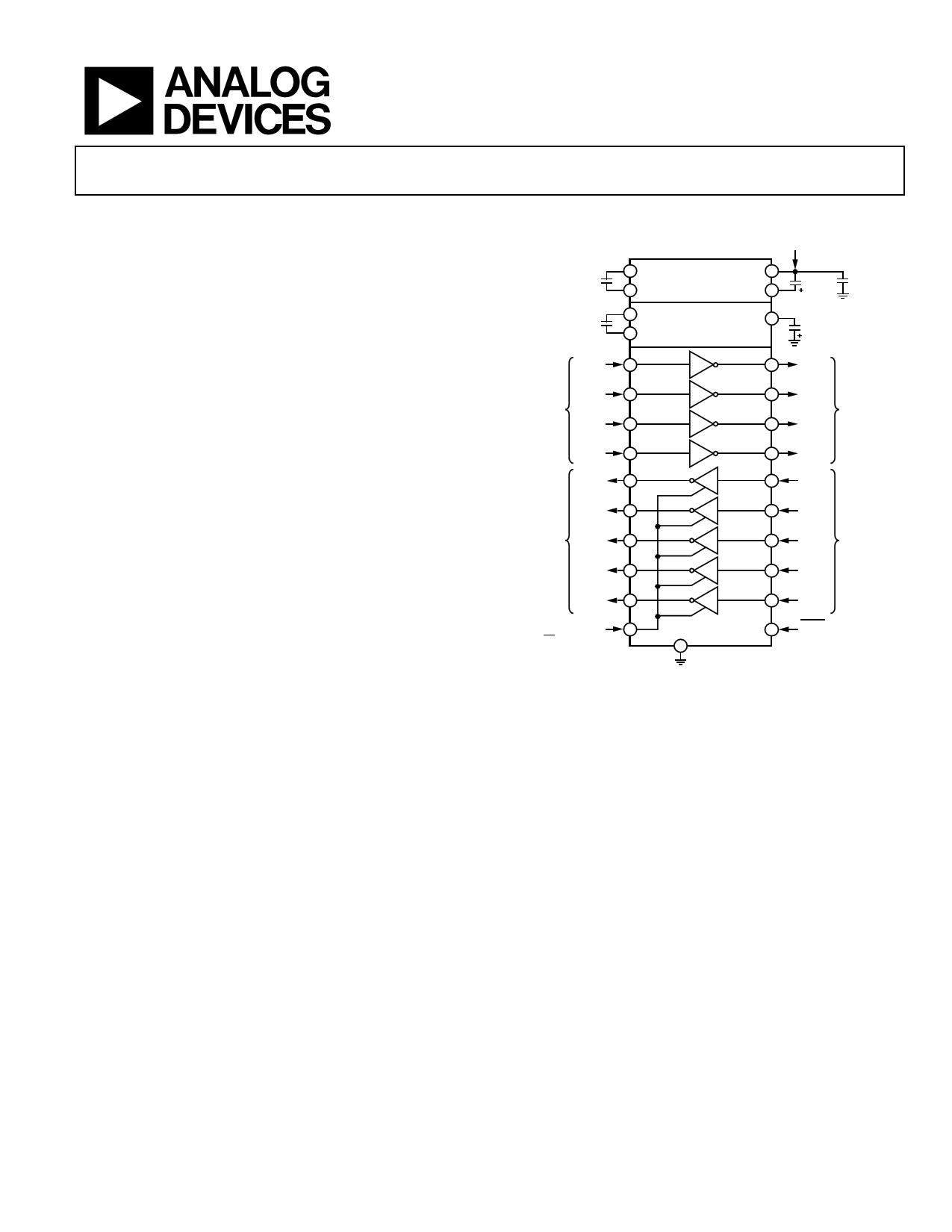
FUNCTIONAL BLOCK DIAGRAM
+3.3V INPUT
1µF +
10V
1µF +
10V
T1IN
12 C1+ +3.3V TO +6.6V
VOLTAGE
14 C1– DOUBLER
VCC 11
V+ 13
15 C2+ +6.6V TO –6.6V
VOLTAGE
16 C2– INVERTER
V– 17
7 T1
2
C3
1µF
6.3V
C4
1µF
10V
T1OUT
0.1µF
CMOS
INPUTS
T2IN
T3IN
6
20
T2
T3
3 T2OUT
EIA/TIA-232
OUTPUTS
1 T3OUT
T4IN
R1OUT
21
8
T4
R1
28 T4OUT
9 R1IN
R2OUT
CMOS
OUTPUTS
R3OUT
R4OUT
5
26
22
R2 4 R2IN
R3
27
R3IN
EIA/TIA-232
INPUTS
R4 23 R4IN
R5OUT
EN (ADM560)
EN (ADM561)
19
24
R5 18
GND
ADM560/
ADM561
25
10
R5IN
SHDN (ADM560)
SHDN (ADM561)
Figure 1.
device begins communication. The active receivers alert the
processor, and then take the ADM560 out of shutdown mode.
The ADM561 features active high shutdown and an active
low receiver enable. In this device, all receivers are disabled
in shutdown.
The ADM560/ADM561 are fabricated using CMOS technology
for minimal power consumption. They feature a high level of
over-voltage protection and latch-up immunity. The receiver
inputs can withstand up to ±25 V levels. The transmitter inputs
can be driven from either 3 V or 5 V logic levels. This allows
operation in mixed 3 V/5 V power supply systems.
The ADM560/ADM561 are packaged in a 28-lead SOIC and
a 28-lead SSOP package.
Rev. B
Information furnished by Analog Devices is believed to be accurate and reliable. However, no
responsibility is assumed by Analog Devices for its use, nor for any infringements of patents or other
rights of third parties that may result from its use. Specifications subject to change without notice. No
license is granted by implication or otherwise under any patent or patent rights of Analog Devices.
Trademarksandregisteredtrademarksarethepropertyoftheirrespectiveowners.
One Technology Way, P.O. Box 9106, Norwood, MA 02062-9106, U.S.A.
Tel: 781.329.4700
www.analog.com
Fax: 781.461.3113
©2006 Analog Devices, Inc. All rights reserved.
1 page 
ADM560/ADM561
PIN CONFIGURATION AND FUNCTION DESCRIPTIONS
T3OUT 1
T1OUT 2
T2OUT 3
R2IN 4
R2OUT 5
T2IN 6
T1IN 7
R1OUT 8
R1IN 9
GND 10
VCC 11
C1+ 12
V+ 13
C1– 14
ADM560
TOP VIEW
(Not to Scale)
28 T4OUT
27 R3IN
26 R3OUT
25 SHDN
24 EN
23 R4IN
22 R4OUT
21 T4IN
20 T3IN
19 R5OUT
18 R5IN
17 V–
16 C2–
15 C2+
Figure 2.ADM560 Pin Configuration
T3OUT 1
T1OUT 2
T2OUT 3
R2IN 4
R2OUT 5
T2IN 6
T1IN 7
R1OUT 8
R1IN 9
GND 10
VCC 11
C1+ 12
V+ 13
C1– 14
ADM561
TOP VIEW
(Not to Scale)
28 T4OUT
27 R3IN
26 R3OUT
25 SHDN
24 EN
23 R4IN
22 R4OUT
21 T4IN
20 T3IN
19 R5OUT
18 R5IN
17 V–
16 C2–
15 C2+
Figure 3. ADM561 Pin Configuration
Table 3. Pin Function Descriptions
Pin No.
Mnemonic
Description
2, 3, 1, 28
T1OUT to T4OUT
9, 4, 27, 23, 18 R1IN to R5IN
Transmitter (Driver) Outputs. Typically ±6 V.
Receiver Inputs. These inputs accept RS-232 signal levels. An internal 5 kΩ pull-down resistor to GND is
connected on each of these inputs.
8, 5, 26, 22, 19 R1OUT to R5OUT
7, 6, 20, 21
T1IN to T4IN
10 GND
Receiver Outputs. These are 3 V logic levels.
Transmitter (Driver) Inputs. These inputs accept 3 V or 5 V logic levels. An internal 400 kΩ pull-up resistor
to VCC is connected on each input.
Ground Pin. Must be connected to 0 V.
11
12, 14
VCC
C1+, C1−
Power Supply Input 3.3 V ± 10%.
External Capacitor 1 is connected between these pins.
13 V+
Internally Generated Positive Supply. +6.6 V nominal.
15, 16
C2+, C2−
External Capacitor 2 is connected between these pins.
17 V−
Internally Generated Negative Supply. −6.6 V nominal.
24
EN/EN
Receiver Enable. EN, active high on ADM560. EN, active low on ADM561. Refer to Table 4.
25 SHDN/SHDN Shutdown Control. SHDN, active low on ADM560. SHDN, active high on ADM561. Refer to Table 4.
Table 4. ADM560/ADM561 Enable and Shutdown Control
ADM560
Normal Operation
SHDN = 1
EN = 1; receivers active
EN = 0; receivers inactive
Shutdown Mode
SHDN = 0
EN = 1; Receiver R1 to Receiver R3 inactive
EN = 1; Receiver R4 and Receiver R5 active
EN = 0; Receiver R1 to Receiver R5 inactive
ADM561
SHDN = 0
EN = 0; receivers active
EN = 1; receivers inactive
SHDN = 1
EN = 0; receivers inactive
EN = 1; receivers inactive
Rev. B | Page 5 of 12
5 Page 
NOTES
ADM560/ADM561
Rev. B | Page 11 of 12
11 Page | ||
| Páginas | Total 12 Páginas | |
| PDF Descargar | [ Datasheet ADM561.PDF ] | |
Hoja de datos destacado
| Número de pieza | Descripción | Fabricantes |
| ADM560 | RS-232 Notebook PC Serial Port Drivers/Receivers | Analog Devices |
| ADM561 | RS-232 Notebook PC Serial Port Drivers/Receivers | Analog Devices |
| Número de pieza | Descripción | Fabricantes |
| SLA6805M | High Voltage 3 phase Motor Driver IC. |
Sanken |
| SDC1742 | 12- and 14-Bit Hybrid Synchro / Resolver-to-Digital Converters. |
Analog Devices |
|
DataSheet.es es una pagina web que funciona como un repositorio de manuales o hoja de datos de muchos de los productos más populares, |
| DataSheet.es | 2020 | Privacy Policy | Contacto | Buscar |