|
|
|
PDF ADUC831BCP Data sheet ( Hoja de datos )
| Número de pieza | ADUC831BCP | |
| Descripción | MicroConverter/ 12-Bit ADCs and DACs with Embedded 62 kBytes Flash MCU | |
| Fabricantes | Analog Devices | |
| Logotipo | ||
Hay una vista previa y un enlace de descarga de ADUC831BCP (archivo pdf) en la parte inferior de esta página. Total 30 Páginas | ||
|
No Preview Available !
MicroConverter®, 12-Bit ADCs and DACs
with Embedded 62 kBytes Flash MCU
ADuC831
FEATURES
ANALOG I/O
8-Channel, 247 kSPS 12-Bit ADC
DC Performance: ؎1 LSB INL
AC Performance: 71 dB SNR
DMA Controller for High Speed ADC-to-RAM Capture
2 12-Bit (Monotonic) Voltage Output DACs
Dual Output PWM/⌺-⌬ DACs
On-Chip Temperature Sensor Function ؎3؇C
On-Chip Voltage Reference
Memory
62 kBytes On-Chip Flash/EE Program Memory
4 kBytes On-Chip Flash/EE Data Memory
Flash/EE, 100 Yr Retention, 100 kCycles Endurance
2304 Bytes On-Chip Data RAM
8051 Based Core
8051 Compatible Instruction Set (16 MHz Max)
12 Interrupt Sources, 2 Priority Levels
Dual Data Pointer
Extended 11-Bit Stack Pointer
On-Chip Peripherals
Time Interval Counter (TIC)
UART, I2C®, and SPI® Serial I/O
Watchdog Timer (WDT), Power Supply Monitor (PSM)
Power
Specified for 3 V and 5 V Operation
Normal, Idle, and Power-Down Modes
Power-Down: 20 A @ 3 V
APPLICATIONS
Optical Networking—Laser Power Control
Base Station Systems
Precision Instrumentation, Smart Sensors
Transient Capture Systems
DAS and Communications Systems
Pin compatible upgrade to existing ADuC812 systems
that require additional code or data memory. Runs
from 1 MHz–16 MHz to external crystal.
The ADuC832 is also available. Functionally is the same
as the ADuC831, except the ADuC832 runs from a 32 kHz
external crystal with on-chip PLL.
MicroConverter is a registered trademark and QuickStart is a trademark
of Analog Devices, Inc.
SPI is a registered trademark of Motorola, Inc.
I2C is a registered trademark of Philips Corporation.
REV. 0
Information furnished by Analog Devices is believed to be accurate and
reliable. However, no responsibility is assumed by Analog Devices for its
use, nor for any infringements of patents or other rights of third parties that
may result from its use. No license is granted by implication or otherwise
under any patent or patent rights of Analog Devices. Trademarks and
registered trademarks are the property of their respective companies.
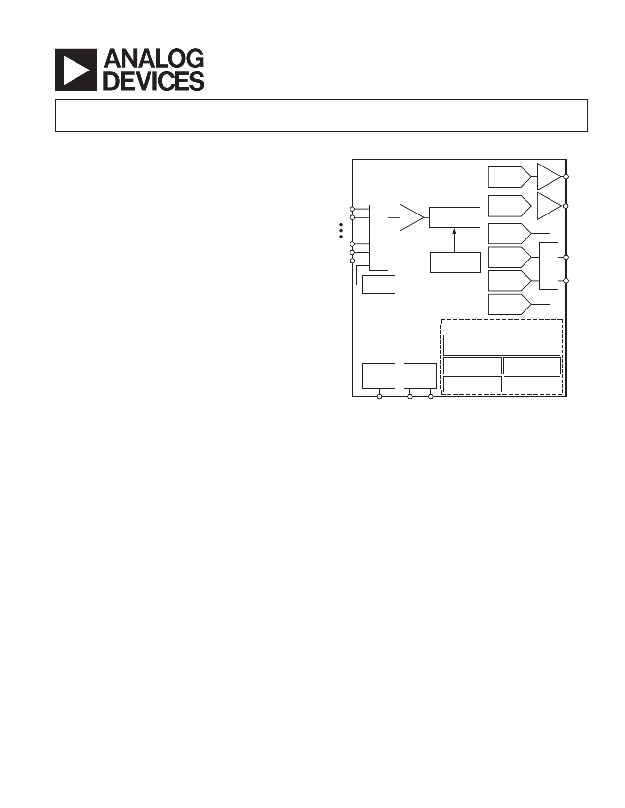
FUNCTIONAL BLOCK DIAGRAM
ADuC831
12-BIT
DAC
BUF
DAC
ADC0
ADC1
ADC5
ADC6
ADC7
MUX
T/H
TEMP
SENSOR
12-BIT ADC
HARDWARE
CALIBRATON
12-BIT
DAC
16-BIT
⌺-⌬ DAC
16-BIT
⌺-⌬ DAC
16-BIT
PWM
16-BIT
PWM
BUF
DAC
MUX
PWM0
PWM1
INTERNAL
BAND GAP
VREF
OSC
8051-BASED MCU WITH ADDITIONAL
PERIPHERALS
62 kBYTES FLASH/EE PROGRAM MEMORY
4 kBYTES FLASH/EE DATA MEMORY
2304 BYTES USER RAM
3 ؋ 16 BIT TIMERS POWER SUPPLY MON
1 ؋ REAL TIME CLOCK WATCHDOG TIMER
PARALLEL
PORTS
UART, I2C, AND SPI
SERIAL I/O
VREF
XTAL1 XTAL2
GENERAL DESCRIPTION
The ADuC831 is a fully integrated 247 kSPS data acquisition
system incorporating a high performance self-calibrating multi-
channel 12-bit ADC, dual 12-bit DACs, and programmable
8-bit MCU on a single chip.
The microcontroller core is an 8052, and therefore 8051-
instruction-set compatible with 12 core clock periods per machine
cycle. 62 kBytes of nonvolatile Flash/EE program memory are
provided on-chip. Four kBytes of nonvolatile Flash/EE data
memory, 256 bytes RAM and 2 kBytes of extended RAM are
also integrated on-chip.
The ADuC831 also incorporates additional analog functionality
with two 12-bit DACs, power supply monitor, and a band gap
reference. On-chip digital peripherals include two 16-bit Σ-∆
DACs, dual output 16-bit PWM, watchdog timer, time interval
counter, three timers/counters, Timer 3 for baud rate generation
and serial I/O ports (I2C, SPI and UART).
On-chip factory firmware supports in-circuit serial download and
debug modes (via UART), as well as single-pin emulation mode
via the EA pin. The ADuC831 is supported by QuickStart™ and
QuickStart Plus development systems featuring low cost software
and hardware development tools. A functional block diagram of
the ADuC831 is shown above with a more detailed block diagram
shown in Figure 1.
The part is specified for 3 V and 5 V operation over the extended
industrial temperature range, and is available in a 52-lead plastic
quad flatpack package and in a 56-lead chip scale package.
One Technology Way, P.O. Box 9106, Norwood, MA 02062-9106, U.S.A.
Tel: 781/329-4700
www.analog.com
Fax: 781/326-8703 © Analog Devices, Inc., 2002. All rights reserved.
1 page 
ADuC831
Parameter
SCLOCK and RESET Only4
(Schmitt-Triggered Inputs)
VT+
VT–
VT+ – VT–
CRYSTAL OSCILLATOR
Logic Inputs, XTAL1 Only
VINL, Input Low Voltage
VINH, Input High Voltage
XTAL1 Input Capacitance
XTAL2 Output Capacitance
MCU CLOCK RATE
DIGITAL OUTPUTS
Output High Voltage (VOH)
VDD = 5 V
1.3
3.0
0.8
1.4
0.3
0.85
0.8
3.5
18
18
16
2.4
4.0
Output Low Voltage (VOL)
ALE, Ports 0 and 2
Port 3
SCLOCK/SDATA
Floating State Leakage Current4
Floating State Output Capacitance
START UP TIME
At Power-On
From Idle Mode
From Power-Down Mode
Wakeup with INT0 Interrupt
Wakeup with SPI/I2C Interrupt
Wakeup with External RESET
After External RESET in Normal Mode
After WDT Reset in Normal Mode
0.4
0.2
0.4
0.4
± 10
±1
10
500
100
150
150
150
30
3
VDD = 3 V
0.95
2.5
0.4
1.1
0.3
0.85
0.4
2.5
18
18
16
2.4
2.6
0.4
0.2
0.4
0.4
± 10
±1
10
500
100
400
400
400
30
3
Unit
V min
V max
V min
V max
V min
V max
V typ
V typ
pF typ
pF typ
MHz max
V min
V typ
V min
V typ
V max
V typ
V max
V max
µA max
µA typ
pF typ
ms typ
µs typ
µs typ
µs typ
µs typ
ms typ
ms typ
Test Conditions/Comments
VDD = 4.5 V to 5.5 V
ISOURCE = 80 µA
VDD = 2.7 V to 3.3 V
ISOURCE = 20 µA
ISINK = 1.6 mA
ISINK = 1.6 mA
ISINK = 4 mA
ISINK = 8 mA, I2C Enabled
MCLKIN = 16 MHz
Controlled via WDCON SFR
REV. 0
–5–
5 Page 
Typical Performance Characteristics–ADuC831
The typical performance plots presented in this section illustrate
typical performance of the ADuC831 under various operating
conditions.
TPC 1 and TPC 2 below show typical ADC Integral Nonlinearity
(INL) errors from ADC code 0 to code 4095 at 5 V and 3 V
supplies respectively. The ADC is using its internal reference
(2.5 V) and operating at a sampling rate of 152 kHz and the
typically worst-case errors in both plots is just less than 0.3 LSBs.
TPC 3 and TPC 4 below show the variation in Worst Case
Positive (WCP) INL and Worst Case Negative (WCN) INL
versus external reference input voltage.
TPC 5 and TPC 6 show typical ADC differential nonlinearity
(DNL) errors from ADC code 0 to code 4095 at 5 V and 3 V sup-
plies, respectively. The ADC is using its internal reference (2. V) and
operating at a sampling rate of 152 kHz and the typically worst case
errors in both plots is just less than 0.2 LSBs.
TPC 7 and TPC 8 show the variation in worst case positive
(WCP) DNL and worst-case negative (WCN) DNL versus
external reference input voltage.
TPC 9 shows a histogram plot of 10,000 ADC conversion
results on a dc input with VDD = 5 V. The plot illustrates an
excellent code distribution pointing to the low noise perfor-
mance of the on-chip precision ADC.
TPC 10 shows a histogram plot of 10,000 ADC conversion
results on a dc input for VDD = 3 V. The plot again illustrates a
very tight code distribution of 1 LSB with the majority of codes
appearing in one output bin.
TPC 11 and TPC 12 show typical FFT plots for the ADuC831.
These plots were generated using an external clock input. The
ADC is using its internal reference (2.5 V) sampling a full-scale,
10 kHz sine wave test tone input at a sampling rate of 149.79 kHz.
The resultant FFTs shown at 5 V and 3 V supplies illustrate an
excellent 100 dB noise floor, 71 dB Signal-to-Noise Ratio (SNR)
and THD greater than –80 dB.
TPC 13 and TPC 14 show typical dynamic performance versus
external reference voltages. Again excellent ac performance can
be observed in both plots with some roll-off being observed as
VREF falls below 1 V.
TPC 15 shows typical dynamic performance versus sampling
frequency. SNR levels of 71 dBs are obtained across the sam-
pling range of the ADuC831.
TPC 16 shows the voltage output of the on-chip temperature
sensor versus temperature. Although the initial voltage output at
25ºC can vary from part to part, the resulting slope of
–2 mV/ºC is constant across all parts.
1.0
0.8
AVDD / DVDD = 5V
fS = 152kHz
0.6
0.4
0.2
0
–0.2
–0.4
–0.6
–0.8
–1.0
0
511 1023 1535 2047 2559 3071 3583 4095
ADC CODES
TPC 1. Typical INL Error, VDD = 5 V
1.2 0.6
AVDD/DVDD = 5V
1.0 fS = 152kHz
0.4
0.8
0.6 0.2
WCP INL
0.4
0
0.2
0 –0.2
–0.2
WCN INL
–0.4
–0.4
–0.6
–0.6
0.5 1.0 1.5 2.0 2.5 5.0
EXTERNAL REFERENCE – V
TPC 3. Typical Worst Case INL Error vs. VREF, VDD = 5 V
1.0
AVDD/DVDD = 3V
0.8 fS = 152kHz
0.6
0.4
0.2
0
–0.2
–0.4
–0.6
–0.8
–1.0
0
511 1023 1535 2047 2559 3071 3583 4095
ADC CODES
TPC 2. Typical INL Error, VDD = 3 V
REV. 0
0.8 0.8
AVDD/DVDD = 3V
0.6
fS = 152kHz
0.6
0.4
WCP INL
0.4
0.2 0.2
00
–0.2
–0.2
–0.4
WCN INL
–0.4
–0.6
–0.6
–0.8 –0.8
0.5 1.0 1.5 2.0 2.5 3.0
EXTERNAL REFERENCE – V
TPC 4. Typical Worst Case INL Error vs. VREF, VDD = 3 V
–11–
11 Page | ||
| Páginas | Total 30 Páginas | |
| PDF Descargar | [ Datasheet ADUC831BCP.PDF ] | |
Hoja de datos destacado
| Número de pieza | Descripción | Fabricantes |
| ADUC831BCP | MicroConverter/ 12-Bit ADCs and DACs with Embedded 62 kBytes Flash MCU | Analog Devices |
| Número de pieza | Descripción | Fabricantes |
| SLA6805M | High Voltage 3 phase Motor Driver IC. |
Sanken |
| SDC1742 | 12- and 14-Bit Hybrid Synchro / Resolver-to-Digital Converters. |
Analog Devices |
|
DataSheet.es es una pagina web que funciona como un repositorio de manuales o hoja de datos de muchos de los productos más populares, |
| DataSheet.es | 2020 | Privacy Policy | Contacto | Buscar |