|
|
|
PDF ADUC814 Data sheet ( Hoja de datos )
| Número de pieza | ADUC814 | |
| Descripción | MicroConverter/ Small Package 12-Bit ADC with Embedded Flash MCU | |
| Fabricantes | Analog Devices | |
| Logotipo | ||
Hay una vista previa y un enlace de descarga de ADUC814 (archivo pdf) en la parte inferior de esta página. Total 30 Páginas | ||
|
No Preview Available !
MicroConverter®, Small Package
12-Bit ADC with Embedded Flash MCU
ADuC814
FEATURES
ANALOG I/O
6-channel 247 kSPS ADC
12-bit resolution
ADC high speed data capture mode
Programmable reference via on-chip DAC for low
level inputs, ADC performance specified to VREF = 1 V
Dual voltage output DACs
12-bit resolution, 15 µs settling time
Memory
8 kbytes on-chip Flash/EE program memory
640 bytes on-chip Flash/EE data memory
Flash/EE, 100 year retention, 100 kcycle endurance
3 levels of Flash/EE program memory security
In-circuit serial downlaod (no external hardware)
256 bytes on-chip data RAM
8051 based core
8051 compatible instruction set
32 kHz external crystal,
on-chip programmable PLL (16.78 MHz max)
Three 16-bit timer/counters
11 programmable I/O lines
11 interrupt sources, 2 priority levels
Power
Specified for 3 V and 5 V operation
Normal: 3 mA @ 3 V (core CLK = 2.1 MHz)
Power-down: 15 µA (32 kHz oscillator running)
On-chip peripherals
Power-on reset circuit (no need for external POR device)
Temperature monitor (±1.5°C accuracy)
Precision voltage reference
Time interval counter (wake-up/RTC timer)
UART serial I/O
SPI®/I2C® compatible serial I/O
Watchdog timer (WDT), power supply monitor (PSM)
Package and temperature range
28-lead TSSOP 4.4 mm × 9.7 mm package
Fully specified for −40°C to +125°C operation
APPLICATIONS
Optical networking—laser power control
Base station systems—power amplifier bias control
Precision instruments, smart sensors
Battery-powered systems, precision system monitors
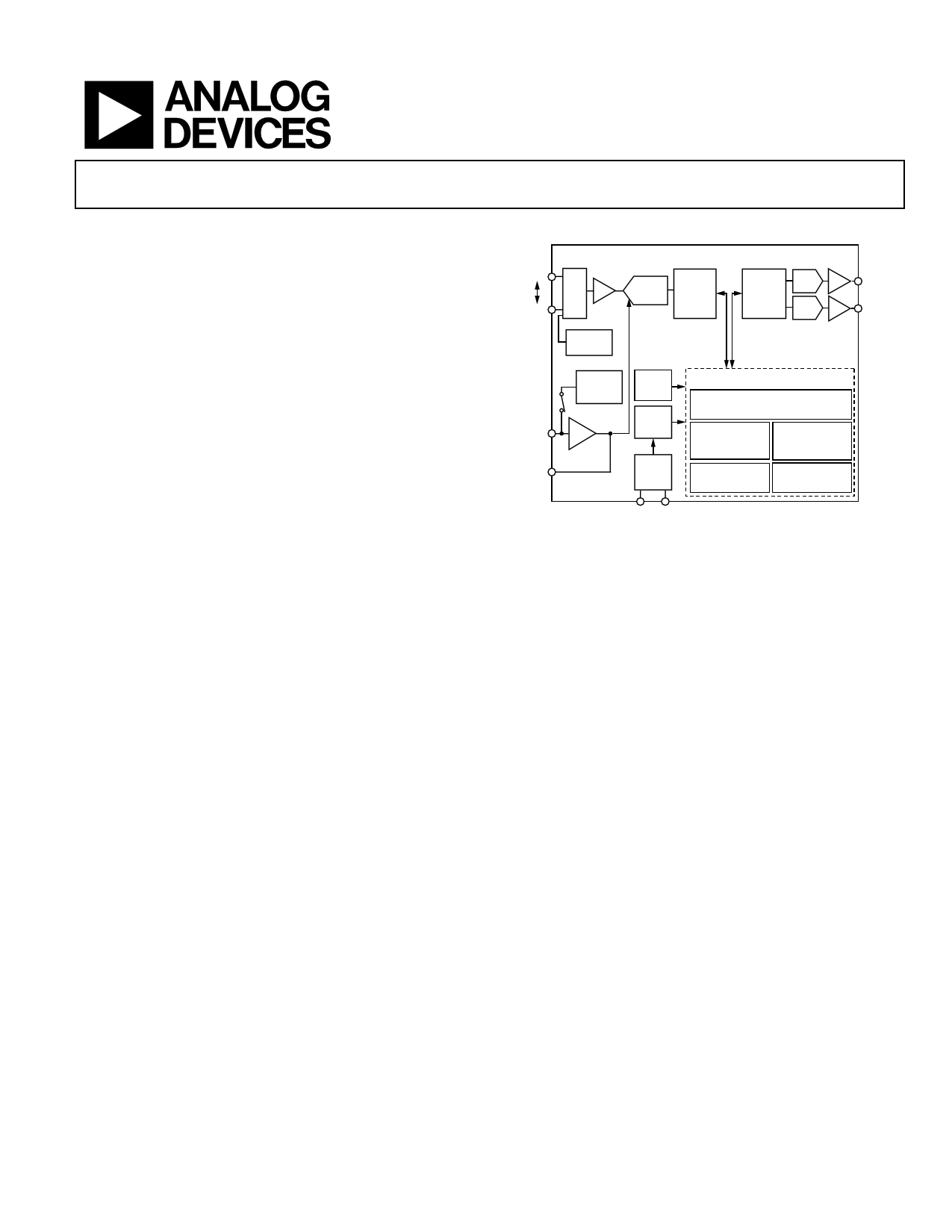
FUNCTIONAL BLOCK DIAGRAM
AIN0
AIN5
AIN
MUX
T/H
ADuC814
12-BIT
ADC
ADC
CONTROL
LOGIC
DAC
CONTROL
LOGIC
DAC0 BUF
DAC1 BUF
DAC0
DAC1
TEMP
MONITOR
VREF
CREF
INTERNAL
BAND GAP
VREF
BUF
POWER-
ON
RESET
PROG.
CLOCK
DIVIDER
OSC
AND
PLL
8051-BASED MCU WITH ADDITIONAL
PERIPHERALS
8 KBYTES FLASH/EE PROGRAM MEMORY
640 BYTES FLASH/EE DATA MEMORY
256 BYTES USER RAM
3 × 16-BIT
TIMER/COUNTERS
1 × WAKE-UP/RTC
TIMER
ON-CHIP MONITORS
POWER SUPPLY
MONITOR
WATCHDOG TIMER
10 × DIGITAL
I/O PINS
UART AND SPI
SERIAL I/O
XTAL1 XTAL2
Figure 1.
GENERAL DESCRIPTION
The ADuC814 is a fully integrated 247 kSPS, 12-bit data acquisi-
tion system incorporating a high performance multichannel
ADC, an 8-bit MCU, and program/data Flash/EE memory on a
single chip.
This low power device operates from a 32 kHz crystal with an
on-chip PLL generating a high frequency clock of 16.78 MHz.
This clock is, in turn, routed through a programmable clock
divider from which the MCU core clock operating frequency is
generated.
The microcontroller core is an 8052 and is compatible with an
8051 instruction. 8 kBytes of nonvolatile Flash/EE program
memory are provided on-chip. 640 bytes of nonvolatile Flash/EE
data memory and 256 bytes RAM are also integrated on-chip.
The ADuC814 also incorporates additional analog functionality
with dual 12-bit DACs, a power supply monitor, and a band gap
reference. On-chip digital peripherals include a watchdog timer,
time interval counter, three timer/counters, and two serial I/O
ports (SPI and UART).
On-chip factory firmware supports in-circuit serial download
and debug modes (via UART), as well as single-pin emulation
mode via the DLOAD pin. The ADuC814 is supported by a
QuickStart™ Development System.
The part operates from a single 3 V or 5 V supply over the
extended temperature range −40°C to +125°C. When operating
from 3 V supplies, the power dissipation for the part is below
10 mW. The ADuC814 is housed in a 28-lead TSSOP package.
Rev. A
Information furnished by Analog Devices is believed to be accurate and reliable.
However, no responsibility is assumed by Analog Devices for its use, nor for any
infringements of patents or other rights of third parties that may result from its use.
Specifications subject to change without notice. No license is granted by implication
or otherwise under any patent or patent rights of Analog Devices. Trademarks and
registered trademarks are the property of their respective owners.
One Technology Way, P.O. Box 9106, Norwood, MA 02062-9106, U.S.A.
Tel: 781.329.4700
www.analog.com
Fax: 781.326.8703 © 2003 Analog Devices, Inc. All rights reserved.
1 page 
Parameter
TEMPERATURE MONITOR9
Voltage Output at 25ºC
Voltage TC
Accuracy
Accuracy
DAC CHANNEL SPECIFICATIONS
DC ACCURACY10
Resolution
Relative Accuracy
Differential Nonlinearity11
Offset Error
Gain Error
Gain Error Mismatch
ANALOG OUTPUTS
Voltage Range_0
Voltage Range_1
Output Impedance
ISINK
DAC AC Specifications
Voltage Output Settling Time
VDD = 5 V
650
–2
3
1.5
12
+3
–1
1/2
50
1
1
0.5
0 to VREF
0 to VDD
0.5
50
15
Digital-to-Analog Glitch Energy
REFERENCE INPUT/OUTPUT
REFERENCE OUTPUT
Output Voltage (VREF)
Accuracy
Power Supply Rejection
Reference Tempco
Internal VREF Power-On Time12
EXTERNAL REFERENCE INPUT13
10
2.5
2.5
47
100
80
Voltage Range (VREF)14
Input Impedance
Input Leakage
POWER SUPPLY MONITOR (PSM)
VDD Trip Point Selection Range
VDD Power Supply Trip Point Accuracy
WATCH DOG TIMER (WDT)14
Timeout Period
LOGIC INPUTS
INPUT VOLTAGES14
All Inputs except SCLOCK, RESET, and
XTAL1
VINL, Input Low Voltage
VINH, Input High Voltage
1.0
VDD
20
10
2.63
2.93
3.08
4.63
3.5
0
2000
0.8
2.0
VDD = 3 V
650
–2
3
1.5
Unit
mV typ
mV/ºC typ
ºC typ
ºC typ
12 Bits
+3 LSB typ
–1 LSB max
1/2 LSB typ
50 mV max
1 % max
1 % typ
0.5 % typ
Volts
Volts
0.5 Ω typ
50 µA typ
15 µs typ
10 nVs typ
2.5
2.5
57
100
80
1.0
VDD
20
10
2.63
2.93
3.08
3.5
0
2000
V
% max
dB typ
ppm/ºC typ
ms typ
V min
V max
kΩ typ
µA max
V
V
V
V
% max
ms min
ms max
0.4 V max
2.0 V min
Test Conditions
ADuC814
2.5 V internal reference
2.5 V external reference
DAC Load to AGND RL = 10 kΩ, CL = 100 pF
Guaranteed montonic
VREF range
VREF range
AVDD range
Of full scale on DAC1
DAC VREF = 2.5 V
DAC VREF = VDD
Full-scale settling time to within ½ LSB of final
value
1 LSB change at major carry
Of VREF measured at the CREF pin
Internal band gap reference deselected via
ADCCON2.6
Four trip points selectable in this range
programmed via TP1–0 in PSMCON
Nine time-out periods selectable in this range
programmed via PRE3–0 in WDCON
Rev. A | Page 5 of 72
5 Page 
ADuC814
Pin No. Mnemonic Type Function
17 CREF
I Decoupling Input for On-Chip Reference. Connect 0.1 µF between this pin and AGND.
18–21 P1.4–P1.7
I
Port 1.4 to P1.7. These pins have no digital output drivers, i.e., they can only function as digital inputs,
for which 0 must be written to the port bit. These port pins also have the following analog functionality:
18 P1.4/ADC2 I ADC Input Channel 2. Selected via ADCCON2 SFR.
19 P1.5/ADC3 I ADC Input Channel 2. Selected via ADCCON2 SFR.
20
P1.6/ADC4/ I/O
ADC Input Channel 4. Selected via ADCCON2 SFR. The voltage DAC Channel 0 can also be configured
DAC0
to appear on P1.6.
21 P1.7/
I/O ADC Input Channel 5, selected via ADCCON2 SFR. The voltage DAC Channel 1 can also be configured
ADC5/DAC1
to appear on P1.7.
22–24 P3.5–P3.7
I/O Bidirectional Port Pins with Internal Pull-Up Resistors. Port 3 pins that have 1s written to them are
pulled high by the internal pull-up resistors, and in that state they can be used as inputs. As inputs
,with Port 3 pins being pulled low externally, they source current because of the internal pull-up
resistors. When driving a 0-to-1 output transition a strong pull-up is active during S1 of the instruction
cycle. Port 3 pins also have various secondary functions which are described as follows.
22 P3.5/T1
I/O Timer/Counter 1 Input. P3.5–P3.7 pins also have SPI interface functions. To enable these functions,
Bit 0 of the CFG814 SFR must be set to 1.
22 P3.5/SS
I/O This pin also functions as the Slave Select input for the SPI interface when the device is operated in
/EXTCLK
slave mode. P3.5 can also function as an input for an external clock. This clock effectively bypasses the
PLL. This function is enabled by setting Bit 1 of the CFG814 SFR.
23 P3.6/MISO I/O SPI Master Input/Slave Output Data Input/Output Pin.
24
P3.7/SDATA/ I/O
SPI Master Output/Slave Input Data Input/Output Pin.
MOSI
25 SCLOCK I/O Serial Clock Pin for SPI Serial Interface Clock.
26 XTAL1
I Input to the Crystal Oscillator Inverter.
27 XTAL2
O Output from the Crystal Oscillator Inverter.
28 DVDD
S Analog Positive Supply Voltage, 3 V or 5 V.
I = Input, O = Output, S = Supply, G - Ground.
The following notes apply to the entire data sheet:
• In bit designation tables, set implies a Logic 1 state, and cleared implies a Logic 0 state, unless otherwise stated.
• Set and cleared also imply that the bit is set or cleared by the ADuC814 hardware, unless otherwise stated.
• User software should not write to reserved or unimplemented bits as they may be used in future products.
Rev. A | Page 11 of 72
11 Page | ||
| Páginas | Total 30 Páginas | |
| PDF Descargar | [ Datasheet ADUC814.PDF ] | |
Hoja de datos destacado
| Número de pieza | Descripción | Fabricantes |
| ADUC812 | MicroConverter/ Multichannel 12-Bit ADC with Embedded FLASH MCU | Analog Devices |
| ADuC812BS | MicroConverter/ Multichannel 12-Bit ADC with Embedded FLASH MCU | Analog Devices |
| ADUC814 | MicroConverter/ Small Package 12-Bit ADC with Embedded Flash MCU | Analog Devices |
| ADUC816 | Dual-Channel 16-Bit ADCs | Analog Devices |
| Número de pieza | Descripción | Fabricantes |
| SLA6805M | High Voltage 3 phase Motor Driver IC. |
Sanken |
| SDC1742 | 12- and 14-Bit Hybrid Synchro / Resolver-to-Digital Converters. |
Analog Devices |
|
DataSheet.es es una pagina web que funciona como un repositorio de manuales o hoja de datos de muchos de los productos más populares, |
| DataSheet.es | 2020 | Privacy Policy | Contacto | Buscar |