|
|
|
PDF ADT14 Data sheet ( Hoja de datos )
| Número de pieza | ADT14 | |
| Descripción | Quad Setpoint/ Programmable Temperature Monitor and Controller | |
| Fabricantes | Analog Devices | |
| Logotipo | ||
Hay una vista previa y un enlace de descarga de ADT14 (archivo pdf) en la parte inferior de esta página. Total 16 Páginas | ||
|
No Preview Available !
a
Quad Setpoint, Programmable
Temperature Monitor and Controller
ADT14
FEATURES
Four Programmable Temperature Setpoints
Programmable Thermal Hysteresis
Accuracy ؎3؇C Typ from –40؇C to +125؇C
Temperature Output Scale Factor = 5 mV/K
Resistor Programmable Temperature Setpoints
5 mA Open-Collector Setpoint Outputs
Internal 2.5 V Reference
600 A Max Quiescent Current at +5 V
APPLICATIONS
Power Supply Monitor and Control System
Multiple Fan Controller System
Workstation Thermal Management System
GENERAL DESCRIPTION
The ADT14 is a temperature sensor and controller that generates
an output voltage proportional to temperature and provides four
temperature trip points. The four trip points, or temperature
setpoints, and their hysteresis are determined by voltage levels set
by the user. An on-chip voltage reference provides an easy method
for setting the temperature trip points.
The ADT14 consists of a bandgap voltage reference combined
with four matched comparators. The reference provides both a
temperature-stable 2.5 V output, and a voltage proportional to
absolute temperature (VPTAT) which has a precise temperature
coefficient of 5 mV/K = 5 mV/(°C +273.15). The VPTAT out-
put is nominally 1.49 V at +25°C. The comparators determine
whether the VPTAT output is above the voltages set up by
external resistive dividers (temperature trip points) and generate
an open-collector output signal when one of their respective
thresholds has been exceeded.
Hysteresis is programmed by a user-selected voltage at the hys-
teresis pin. This voltage adjusts the hysteresis current which is
used to generate a hysteresis offset voltage. The comparator’s
noninverting inputs are connected in parallel, which guarantees
that there is no hysteresis overlap and eliminates erratic transi-
tions between adjacent trip zones.
Using a proprietary thin-film resistor process in conjunction
with production laser trimming, a temperature accuracy of ± 3°C
at 25°C is guaranteed. The open-collector outputs are capable
of sinking 5 mA, and provide TTL/CMOS logic compatibility
with an external pull-up resistor. Operating from a single 5 V
supply, the quiescent current is 600 µA max.
The ADT14 is available in the 16-lead epoxy DIP and SO
(small outline) packages.
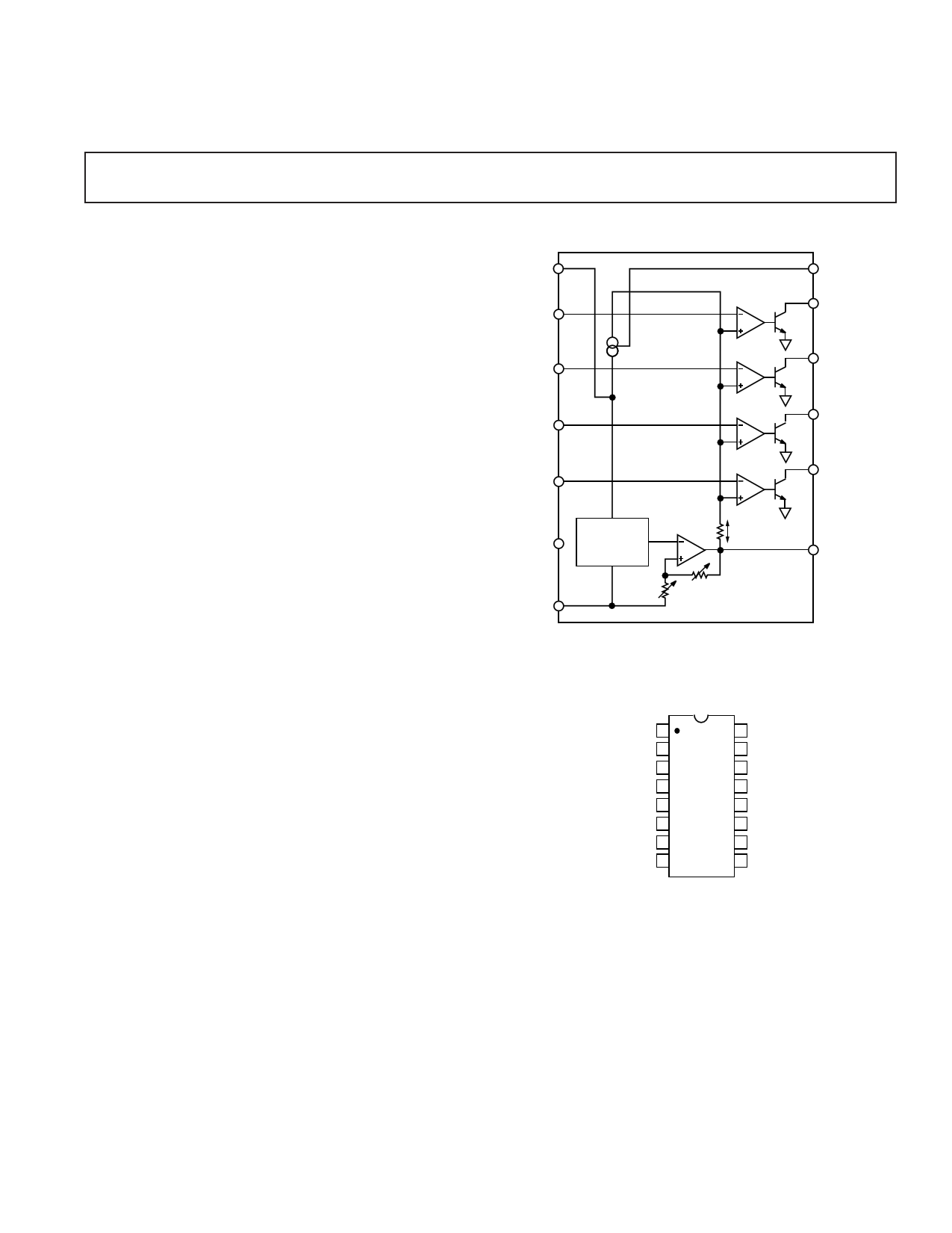
FUNCTIONAL BLOCK DIAGRAM
2.5V
VREF
SET 1
SET 2
CURRENT
MIRROR
HYSTERESIS
SETPOINT
OUTPUT 1
SETPOINT
OUTPUT 2
SET 3
SET 4
WINDOW
COMPARATORS
SETPOINT
OUTPUT 3
SETPOINT
OUTPUT 4
VOLTAGE
V+
REFERENCE
AND
SENSOR
GND
HYSTERESIS
VOLTAGE
TEMPERATURE
OUTPUT
VPTAT
ADT14
PIN CONFIGURATIONS
DIP & SO
OUTPUT 1 1
16 OUTPUT 4
SETPOINT 1 2
15 SETPOINT 4
NC 3
14 2.5V REFERENCE
NC 4 ADT14 13 V+
TOP VIEW
GROUND 5 (Not to Scale) 12 NC
VPTAT 6
11 HYSTERESIS
SETPOINT 2 7
10 SETPOINT 3
OUTPUT 2 8
9 OUTPUT 3
NC = NO CONNECT
REV. 0
Information furnished by Analog Devices is believed to be accurate and
reliable. However, no responsibility is assumed by Analog Devices for its
use, nor for any infringements of patents or other rights of third parties
which may result from its use. No license is granted by implication or
otherwise under any patent or patent rights of Analog Devices.
One Technology Way, P.O. Box 9106, Norwood, MA 02062-9106, U.S.A.
Tel: 617/329-4700 World Wide Web Site: http://www.analog.com
Fax: 617/326-8703
© Analog Devices, Inc., 1997
1 page 
500
475
450
425
400
375
350
325
300
75
V+ = +5V, NO LOAD
25 25
75 125
TEMPERATURE – °C
175
Figure 8. Supply Current vs. Temperature
ADT14
2.52
2.515
2.51
2.505
2.5
2.495
2.49
2.485
2.48
75
MAX LIMIT
V+ = +5V, NO LOAD
MIN LIMIT
25 25
75 125
TEMPERATURE – °C
175
Figure 11. Reference Voltage vs. Temperature
40
35
30
25
20
15
10
5
0
75
VOL = +1V, V+ = +5V
25 25
75 125
TEMPERATURE – °C
175
Figure 9. Open-Collector Output Sink Current vs.
Temperature
0.1
0.075
V+ = +4.5V TO +13V
NO LOAD
0.05
0.025
0
50 25 0
25 50 75 100 125 150
TEMPERATURE – °C
Figure 12. VPTAT Power Supply Rejection vs. Temperature
700
V+ = +5V, NO LOAD
600
500 ILOAD = 5mA
400
300
200 ILOAD = 1mA
100
0
75
25 25
75 125
TEMPERATURE – °C
175
Figure 10. Open-Collector Output Voltage vs. Temperature
2.5V
VLOAD
100
90
0V
VREF
10
0%
500µs
20mV
Figure 13. VREF Under Load Switching (0 µA–500 µA),
RLOAD = 5 kΩ
REV. 0
–5–
5 Page 
ADT14
Buffering the Temperature Output Pin
The VPTAT sensor output is a low impedance dc output volt-
age with a 5 mV/K temperature coefficient, and is useful in a
number of measurement and control applications. In many
applications, this voltage may need to be transmitted to a central
location for processing. The unbuffered VPTAT voltage output
is capable of 500 µA drive into 50 pF (max). As mentioned in
the discussion regarding buffering circuits for the VREF output, it
is useful to consider external amplifiers for interfacing VPTAT
to external circuitry to ensure accuracy, and to minimize load-
ing, which could create dissipation-induced temperature sensing
errors. An excellent general-purpose buffer circuit using the
OP177, which is capable of driving over 10 mA and will remain
stable under capacitive loads of up to 0.1 µF, is shown in Figure
20. Other interface circuits are shown below.
ADT14
VPTAT
10kΩ
0.1 F
V+
100Ω
OP177
V–
VOUT
Figure 20. Buffer VPTAT to Handle Difficult Loads
Differential Transmitter
In noisy industrial environments, it is difficult to send an accu-
rate analog signal over a significant distance. However, by send-
ing the signal differentially on a wire pair, these errors can be
significantly reduced. Since the noise will be picked up equally
on both wires, a receiver with high common-mode input rejec-
tion can be used very effectively to cancel out the noise at the
receiving end. Figure 21 shows two amplifiers being used to
send the signal differentially, and an excellent differential re-
ceiver, the AMP03, (SSM2141 or SSM2143 are two other
options), which features a common-mode rejection ratio of
95 dB at dc and very low input and drift errors.
4.9kΩ
ADT14
VPTAT
10kΩ
50Ω
1/2 OP297
10kΩ
V+
50Ω
1/2 OP297
V–
V+
VOUT
AMP03 OR
SSM2143
V–
Figure 21. Send the Signal Differentially for Noise
Immunity
4 mA to 20 mA Current Loop
Another very common method of transmitting a signal over long
distances is to use a 4 mA-to-20 mA loop (see Figure 22). An
advantage of using a 4 mA-to-20 mA loop is that the accuracy of
a current loop is not compromised by voltage drops across the
line. One requirement of 4 mA-to-20 mA circuits is that the
remote end must receive all of its power from the loop, meaning
that the circuit must consume less than 4 mA. Operating from
+5 V, the quiescent current of the ADT14 is 600 µA max, and
the OP90s is 20 µA max, totaling much less than 4 mA. Although
not shown, the open collector outputs and temperature setting
pins can be connected to do any local control of switching.
The current is proportional to the voltage on the VPTAT out-
put, and is calibrated to 4 mA at a temperature of –40°C, to
20 mA for +85°C. The main equation governing the operation
of this circuit gives the current as a function of VPTAT:
IOUT
=
1 VPTAT × R5
R6 R2
−
V REF × R3
R3 + R1
×
1
+
R5
R2
R1
243kΩ
R3
100kΩ
14 13
VREF
V+
ADT14
56
GND
VPTAT
+5V TO +13.2V
R2
39.2kΩ
27
OP90
34
6
2N1711
R5
100kΩ
R6
100Ω
4-20mA
RL
Figure 22. 4 mA to 20 mA Current Loop
To determine the resistor values in this circuit, first note that
VREF remains constant over temperature. Thus the ratio of R5
over R2 must give a variation of IOUT from 4 mA to 20 mA as
VPTAT varies from 1.165 V at –40°C to 1.79 V at +85°C. The
absolute value of the resistors is not important, only the ratio.
For convenience, 100 kΩ is chosen for R5. Once R2 is calcu-
lated, the value of R3 and R1 is determined by substituting
4 mA for IOUT and 1.165 V for VPTAT and solving. The final
values are shown in the circuit. The OP90 is chosen for this
circuit because of its ability to operate on a single supply and its
high accuracy. For initial accuracy, a 10 kΩ trim potentiometer
can be included in series with R3, and the value of R3 lowered
to 95 kΩ. The potentiometer should be adjusted to produce an
output current of 12.3 mA at 25°C.
Temperature-to-Frequency Converter
Another common method of transmitting analog information is
to convert a voltage to the frequency domain. This is easily done
with any of the available low cost monolithic Voltage-to-Fre-
quency Converters (VFCs) that feature an open-collector digital
output. A digital signal is immune to noise and voltage drops
because the only important information is the frequency. As
long as the conversions between temperature and frequency are
accurately performed, the temperature data can be accurately
transmitted.
A simple circuit to do this combines the ADT14 with an AD654
VFC and is shown in Figure 23. The AD654 outputs a square
wave that is proportional to the dc input voltage according to
the following equation:
FOUT
= V IN
10 (R1+ R2) CT
REV. 0
–11–
11 Page | ||
| Páginas | Total 16 Páginas | |
| PDF Descargar | [ Datasheet ADT14.PDF ] | |
Hoja de datos destacado
| Número de pieza | Descripción | Fabricantes |
| ADT1-1 | RF Transformer | Mini-Circuits |
| ADT1-1+ | RF Transformer | Mini-Circuits |
| ADT1-1WT | RF XFMR / SURF MOUNT /T&R/RoHS | Mini-Circuits |
| ADT1-1WT+ | RF XFMR / SURF MOUNT /T&R/RoHS | Mini-Circuits |
| Número de pieza | Descripción | Fabricantes |
| SLA6805M | High Voltage 3 phase Motor Driver IC. |
Sanken |
| SDC1742 | 12- and 14-Bit Hybrid Synchro / Resolver-to-Digital Converters. |
Analog Devices |
|
DataSheet.es es una pagina web que funciona como un repositorio de manuales o hoja de datos de muchos de los productos más populares, |
| DataSheet.es | 2020 | Privacy Policy | Contacto | Buscar |