|
|
|
PDF ADSP-2189M Data sheet ( Hoja de datos )
| Número de pieza | ADSP-2189M | |
| Descripción | DSP Microcomputer | |
| Fabricantes | Analog Devices | |
| Logotipo | ||
Hay una vista previa y un enlace de descarga de ADSP-2189M (archivo pdf) en la parte inferior de esta página. Total 30 Páginas | ||
|
No Preview Available !
a
DSP Microcomputer
ADSP-2189M
FEATURES
PERFORMANCE
13.3 ns Instruction Cycle Time @ 2.5 Volts (Internal),
75 MIPS Sustained Performance
Single-Cycle Instruction Execution
Single-Cycle Context Switch
3-Bus Architecture Allows Dual Operand Fetches in
Every Instruction Cycle
Multifunction Instructions
Power-Down Mode Featuring Low CMOS Standby
Power Dissipation with 200 CLKIN Cycle Recovery
from Power-Down Condition
Low Power Dissipation in Idle Mode
INTEGRATION
ADSP-2100 Family Code Compatible (Easy to Use Alge-
braic Syntax), with Instruction Set Extensions
192K Bytes of On-Chip RAM, Configured as 32K Words
On-Chip Program Memory RAM and 48K Words On-
Chip Data Memory RAM
Dual Purpose Program Memory for Both Instruction
and Data Storage
Independent ALU, Multiplier/Accumulator and Barrel
Shifter Computational Units
Two Independent Data Address Generators
Powerful Program Sequencer Provides Zero Overhead
Looping Conditional Instruction Execution
Programmable 16-Bit Interval Timer with Prescaler
100-Lead LQFP
SYSTEM INTERFACE
Flexible I/O Structure Allows 2.5 V or 3.3 V Operation;
All Inputs Tolerate Up to 3.6 V, Regardless of Mode
16-Bit Internal DMA Port for High Speed Access to On-
Chip Memory (Mode Selectable)
4 MByte Memory Interface for Storage of Data Tables
and Program Overlays (Mode Selectable)
8-Bit DMA to Byte Memory for Transparent Program
and Data Memory Transfers (Mode Selectable)
I/O Memory Interface with 2048 Locations Supports
Parallel Peripherals (Mode Selectable)
Programmable Memory Strobe and Separate I/O
Memory Space Permits “Glueless” System Design
Programmable Wait-State Generation
Two Double-Buffered Serial Ports with Companding
Hardware and Automatic Data Buffering
Automatic Booting of On-Chip Program Memory from
Byte-Wide External Memory, e.g., EPROM, or
Through Internal DMA Port
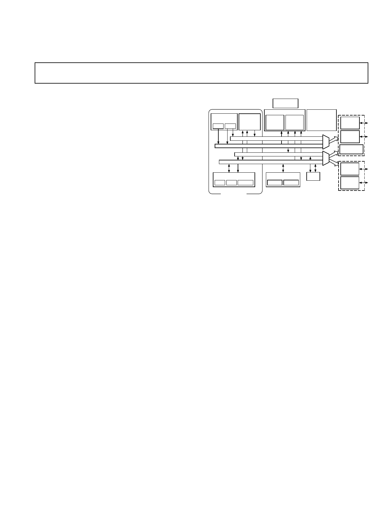
FUNCTIONAL BLOCK DIAGRAM
DATA ADDRESS
GENERATORS PROGRAM
SEQUENCER
DAG 1 DAG 2
POWER-DOWN
CONTROL
MEMORY
PROGRAM
MEMORY
32K ؋
24 BIT
DATA
MEMORY
48K ؋
16 BIT
PROGRAM MEMORY ADDRESS
DATA MEMORY ADDRESS
PROGRAM MEMORY DATA
DATA MEMORY DATA
ARITHMETIC UNITS
ALU MAC SHIFTER
ADSP-2100 BASE
ARCHITECTURE
SERIAL PORTS
SPORT 0 SPORT 1
PROGRAMMABLE
I/O
AND
FLAGS
FULL MEMORY
MODE
EXTERNAL
ADDRESS
BUS
EXTERNAL
DATA
BUS
BYTE DMA
CONTROLLER
TIMER
OR
EXTERNAL
DATA
BUS
INTERNAL
DMA
PORT
HOST MODE
Six External Interrupts
13 Programmable Flag Pins Provide Flexible System
Signaling
UART Emulation through Software SPORT Reconfiguration
ICE-Port™ Emulator Interface Supports Debugging in
Final Systems
GENERAL DESCRIPTION
The ADSP-2189M is a single-chip microcomputer optimized
for digital signal processing (DSP) and other high speed nu-
meric processing applications.
The ADSP-2189M combines the ADSP-2100 family base archi-
tecture (three computational units, data address generators and
a program sequencer) with two serial ports, a 16-bit internal
DMA port, a byte DMA port, a programmable timer, Flag I/O,
extensive interrupt capabilities, and on-chip program and data
memory.
The ADSP-2189M integrates 192K bytes of on-chip memory
configured as 32K words (24-bit) of program RAM and 48K
words (16-bit) of data RAM. Power-down circuitry is also pro-
vided to meet the low power needs of battery operated portable
equipment. The ADSP-2189M is available in a 100-lead LQFP
package.
In addition, the ADSP-2189M supports new instructions, which
include bit manipulations—bit set, bit clear, bit toggle, bit test—
new ALU constants, new multiplication instruction (x squared),
biased rounding, result free ALU operations, I/O memory trans-
fers and global interrupt masking, for increased flexibility.
ICE-Port is a trademark of Analog Devices, Inc.
REV. A
Information furnished by Analog Devices is believed to be accurate and
reliable. However, no responsibility is assumed by Analog Devices for its
use, nor for any infringements of patents or other rights of third parties
which may result from its use. No license is granted by implication or
otherwise under any patent or patent rights of Analog Devices.
One Technology Way, P.O. Box 9106, Norwood, MA 02062-9106, U.S.A.
Tel: 781/329-4700 World Wide Web Site: http://www.analog.com
Fax: 781/326-8703
© Analog Devices, Inc., 2000
1 page 
ADSP-2189M
Table I. Interrupt Priority and Interrupt Vector Addresses
Source Of Interrupt
Interrupt Vector
Address (Hex)
RESET (or Power-Up with PUCR = 1) 0000 (Highest Priority)
Power-Down (Nonmaskable)
IRQ2
IRQL1
IRQL0
002C
0004
0008
000C
SPORT0 Transmit
0010
SPORT0 Receive
IRQE
0014
0018
BDMA Interrupt
SPORT1 Transmit or IRQ1
SPORT1 Receive or IRQ0
001C
0020
0024
Timer
0028 (Lowest Priority)
Interrupt routines can either be nested with higher priority
interrupts taking precedence or processed sequentially. Inter-
rupts can be masked or unmasked with the IMASK register.
Individual interrupt requests are logically ANDed with the bits
in IMASK; the highest priority unmasked interrupt is then
selected. The power-down interrupt is nonmaskable.
The ADSP-2189M masks all interrupts for one instruction cycle
following the execution of an instruction that modifies the IMASK
register. This does not affect serial port autobuffering or DMA
transfers.
The interrupt control register, ICNTL, controls interrupt nest-
ing and defines the IRQ0, IRQ1 and IRQ2 external interrupts to
be either edge- or level-sensitive. The IRQE pin is an external
edge-sensitive interrupt and can be forced and cleared. The
IRQL0 and IRQL1 pins are external level-sensitive interrupts.
The IFC register is a write-only register used to force and clear
interrupts. On-chip stacks preserve the processor status and are
automatically maintained during interrupt handling. The stacks
are twelve levels deep to allow interrupt, loop and subroutine
nesting. The following instructions allow global enable or dis-
able servicing of the interrupts (including power-down), regard-
less of the state of IMASK. Disabling the interrupts does not
affect serial port autobuffering or DMA.
ENA INTS;
DIS INTS;
When the processor is reset, interrupt servicing is enabled.
LOW POWER OPERATION
The ADSP-2189M has three low power modes that significantly
reduce the power dissipation when the device operates under
standby conditions. These modes are:
• Power-Down
• Idle
• Slow Idle
The CLKOUT pin may also be disabled to reduce external
power dissipation.
Power-Down
The ADSP-2189M processor has a low power feature that lets
the processor enter a very low power dormant state through
hardware or software control. Here is a brief list of power-
down features. Refer to the ADSP-2100 Family User’s Manual,
Third Edition, “System Interface” chapter, for detailed infor-
mation about the power-down feature.
• Quick recovery from power-down. The processor begins
executing instructions in as few as 200 CLKIN cycles.
• Support for an externally generated TTL or CMOS proces-
sor clock. The external clock can continue running during
power-down without affecting the lowest power rating and
200 CLKIN cycle recovery.
• Support for crystal operation includes disabling the oscillator
to save power (the processor automatically waits approxi-
mately 4096 CLKIN cycles for the crystal oscillator to start
or stabilize) and letting the oscillator run to allow 200 CLKIN
cycle start up.
• Power-down is initiated by either the power-down pin
(PWD) or the software power-down force bit. Interrupt
support allows an unlimited number of instructions to be
executed before optionally powering down. The power-down
interrupt also can be used as a nonmaskable, edge-sensitive
interrupt.
• Context clear/save control allows the processor to continue
where it left off or start with a clean context when leaving the
power-down state.
• The RESET pin also can be used to terminate power-down.
• Power-down acknowledge pin indicates when the processor
has entered power-down.
Idle
When the ADSP-2189M is in the Idle Mode, the processor
waits indefinitely in a low power state until an interrupt occurs.
When an unmasked interrupt occurs, it is serviced; execution
then continues with the instruction following the IDLE instruc-
tion. In Idle mode IDMA, BDMA and autobuffer cycle steals
still occur.
Slow Idle
The IDLE instruction is enhanced on the ADSP-2189M to let
the processor’s internal clock signal be slowed, further reducing
power consumption. The reduced clock frequency, a program-
mable fraction of the normal clock rate, is specified by a select-
able divisor given in the IDLE instruction.
The format of the instruction is:
IDLE (n);
where n = 16, 32, 64 or 128. This instruction keeps the proces-
sor fully functional, but operating at the slower clock rate. While
it is in this state, the processor’s other internal clock signals,
such as SCLK, CLKOUT and timer clock, are reduced by the
same ratio. The default form of the instruction, when no clock
divisor is given, is the standard IDLE instruction.
When the IDLE (n) instruction is used, it effectively slows down
the processor’s internal clock and thus its response time to in-
coming interrupts. The one-cycle response time of the standard
idle state is increased by n, the clock divisor. When an enabled
interrupt is received, the ADSP-2189M will remain in the idle
state for up to a maximum of n processor cycles (n = 16, 32, 64,
or 128) before resuming normal operation.
When the IDLE (n) instruction is used in systems that have an
externally generated serial clock (SCLK), the serial clock rate
may be faster than the processor’s reduced internal clock rate.
Under these conditions, interrupts must not be generated at a
REV. A
–5–
5 Page 
ADSP-2189M
The IDMA port has a 16-bit multiplexed address and data bus
and supports 24-bit program memory. The IDMA port is com-
pletely asynchronous and can be written while the ADSP-2189M
is operating at full speed.
The DSP memory address is latched and then automatically
incremented after each IDMA transaction. An external device
can therefore access a block of sequentially addressed memory
by specifying only the starting address of the block. This in-
creases throughput as the address does not have to be sent for
each memory access.
IDMA Port access occurs in two phases. The first is the IDMA
Address Latch cycle. When the acknowledge is asserted, a 14-bit
address and 1-bit destination type can be driven onto the bus by
an external device. The address specifies an on-chip memory
location, the destination type specifies whether it is a DM or
PM access. The falling edge of the IDMA address latch signal
(IAL) or the missing edge of the IDMA select signal (IS) latches
this value into the IDMAA register.
Once the address is stored, data can then be either read from, or
written to, the ADSP-2189M’s on-chip memory. Asserting the
select line (IS) and the appropriate read or write line (IRD and
IWR respectively) signals the ADSP-2189M that a particular
transaction is required. In either case, there is a one-processor-
cycle delay for synchronization. The memory access consumes
one additional processor cycle.
Once an access has occurred, the latched address is automati-
cally incremented and another access can occur.
Through the IDMAA register, the DSP can also specify the
starting address and data format for DMA operation. Asserting
the IDMA port select (IS) and address latch enable (IAL) di-
rects the ADSP-2189M to write the address onto the IAD0-14
bus into the IDMA Control Register. If Bit 15 is set to 0, IDMA
latches the address. If Bit 15 is set to 1, IDMA latches into the
OVLAY register. This register, shown below, is memory
mapped at address DM (0x3FE0). Note that the latched address
(IDMAA) cannot be read back by the host.
Refer to the following figures for more information on IDMA
and DMA memory maps.
IDMA OVERLAY
15 14 13 12 11 10 9 8 7 6 5 4 3 2 1 0
0 0 0 0 0 0 0 0 0 0 0 0 0 0 0 DM(0؋3FE7)
RESERVED SET TO 0 ID DMOVLAY ID PMOVLAY
IDMA CONTROL (U = UNDEFINED AT RESET)
15 14 13 12 11 10 9 8 7 6 5 4 3 2 1
UUUU UUUU UUUUUU
0
U DM(0؋3FE0)
IDMAA ADDRESS
IDMAD DESTINATION MEMORY TYPE:
0 = PM
1 = DM
Figure 10. IDMA Control/OVLAY Registers
DMA
DATA MEMORY
OVLAY
DMA
PROGRAM MEMORY
OVLAY
ALWAYS
ACCESSIBLE
AT ADDRESS
ALWAYS
0؋2000 – 0؋3FFF
ACCESSIBLE
AT ADDRESS
0؋0000 – 0؋1FFF
0؋2000–
ACCESSIBLE WHEN
DMOVLAY = 0
0؋0000–
0؋1FFF
0؋0000–
0؋1FFF
ACCPAPEMMSCOSCOVIEVBLASLALCSAEYCIYBWE=L=S0HE4SEWIBNHLEE0NW؋H300FE؋؋FN23F0F000F؋؋0F–230F0F0FAD–CMCOEVADSLCMSACIOYBEVL=ADSLECMS4AWCIOYBEHVL=SLEE5SANWIYBHL=EE6NWH00E؋؋N010F0F000F؋؋–010F0F000F–؋؋010F0F0F–
PMOVLAY = 5
ACCESSIBLE WHEN
NOTE: IDMA AND BDMA HAVEN SEPARATE
DMOVLAY = 7
DMA CONTROL REGISTERS
Figure 11. Direct Memory Access—PM and DM Memory
Maps
Bootstrap Loading (Booting)
The ADSP-2189M has two mechanisms to allow automatic
loading of the internal program memory after reset. The method
for booting is controlled by the Mode A, B and C configuration
bits.
When the MODE pins specify BDMA booting, the ADSP-2189M
initiates a BDMA boot sequence when reset is released.
The BDMA interface is set up during reset to the following
defaults when BDMA booting is specified: the BDIR, BMPAGE,
BIAD and BEAD registers are set to 0, the BTYPE register is
set to 0 to specify program memory 24-bit words, and the
BWCOUNT register is set to 32. This causes 32 words of on-
chip program memory to be loaded from byte memory. These
32 words are used to set up the BDMA to load in the remaining
program code. The BCR bit is also set to 1, which causes pro-
gram execution to be held off until all 32 words are loaded into
on-chip program memory. Execution then begins at address 0.
The ADSP-2100 Family development software (Revision 5.02
and later) fully supports the BDMA booting feature and can
generate byte memory space compatible boot code.
The IDLE instruction can also be used to allow the processor to
hold off execution while booting continues through the BDMA
interface. For BDMA accesses while in Host Mode, the ad-
dresses to boot memory must be constructed externally to the
ADSP-2189M. The only memory address bit provided by the
processor is A0.
IDMA Port Booting
The ADSP-2189M can also boot programs through its Internal
DMA port. If Mode C = 1, Mode B = 0, and Mode A = 1, the
ADSP-2189M boots from the IDMA port. IDMA feature can
load as much on-chip memory as desired. Program execution is
held off until on-chip program memory location 0 is written to.
REV. A
–11–
11 Page | ||
| Páginas | Total 30 Páginas | |
| PDF Descargar | [ Datasheet ADSP-2189M.PDF ] | |
Hoja de datos destacado
| Número de pieza | Descripción | Fabricantes |
| ADSP-2189 | DSP Microcomputer | Analog Devices |
| ADSP-2189M | DSP Microcomputer | Analog Devices |
| ADSP-2189MBST-266 | DSP Microcomputer | Analog Devices |
| ADSP-2189MKST-300 | DSP Microcomputer | Analog Devices |
| Número de pieza | Descripción | Fabricantes |
| SLA6805M | High Voltage 3 phase Motor Driver IC. |
Sanken |
| SDC1742 | 12- and 14-Bit Hybrid Synchro / Resolver-to-Digital Converters. |
Analog Devices |
|
DataSheet.es es una pagina web que funciona como un repositorio de manuales o hoja de datos de muchos de los productos más populares, |
| DataSheet.es | 2020 | Privacy Policy | Contacto | Buscar |