|
|
|
PDF ADSP-2186L Data sheet ( Hoja de datos )
| Número de pieza | ADSP-2186L | |
| Descripción | DSP Microcomputer | |
| Fabricantes | Analog Devices | |
| Logotipo | ||
Hay una vista previa y un enlace de descarga de ADSP-2186L (archivo pdf) en la parte inferior de esta página. Total 30 Páginas | ||
|
No Preview Available !
a
DSP Microcomputer
ADSP-2186L
FEATURES
Performance
25 ns Instruction Cycle Time 40 MIPS Sustained
Performance
Single-Cycle Instruction Execution
Single-Cycle Context Switch
3-Bus Architecture Allows Dual Operand Fetches in
Every Instruction Cycle
Multifunction Instructions
Power-Down Mode Featuring Low CMOS Standby
Power Dissipation with 400 Cycle Recovery from
Power-Down Condition
Low Power Dissipation in Idle Mode
Integration
ADSP-2100 Family Code Compatible, with Instruction
Set Extensions
40K Bytes of On-Chip RAM, Configured as
8K Words On-Chip Program Memory RAM and
8K Words On-Chip Data Memory RAM
Dual Purpose Program Memory for Both Instruction
and Data Storage
Independent ALU, Multiplier/Accumulator and Barrel
Shifter Computational Units
Two Independent Data Address Generators
Powerful Program Sequencer Provides
Zero Overhead Looping Conditional Instruction
Execution
Programmable 16-Bit Interval Timer with Prescaler
100-Lead LQFP and 144-Ball Mini-BGA
System Interface
16-Bit Internal DMA Port for High Speed Access to
On-Chip Memory (Mode Selectable)
4 MByte Byte Memory Interface for Storage of Data
Tables and Program Overlays
8-Bit DMA to Byte Memory for Transparent Program
and Data Memory Transfers (Mode Selectable)
I/O Memory Interface with 2048 Locations Supports
Parallel Peripherals (Mode Selectable)
Programmable Memory Strobe and Separate I/O Memory
Space Permits “Glueless” System Design
(Mode Selectable)
Programmable Wait State Generation
Two Double-Buffered Serial Ports with Companding
Hardware and Automatic Data Buffering
Automatic Booting of On-Chip Program Memory from
Byte-Wide External Memory, e.g., EPROM, or
Through Internal DMA Port
Six External Interrupts
ICE-Port is a trademark of Analog Devices, Inc.
All other trademarks are the property of their respective holders.
REV. B
Information furnished by Analog Devices is believed to be accurate and
reliable. However, no responsibility is assumed by Analog Devices for its
use, nor for any infringements of patents or other rights of third parties
which may result from its use. No license is granted by implication or
otherwise under any patent or patent rights of Analog Devices.
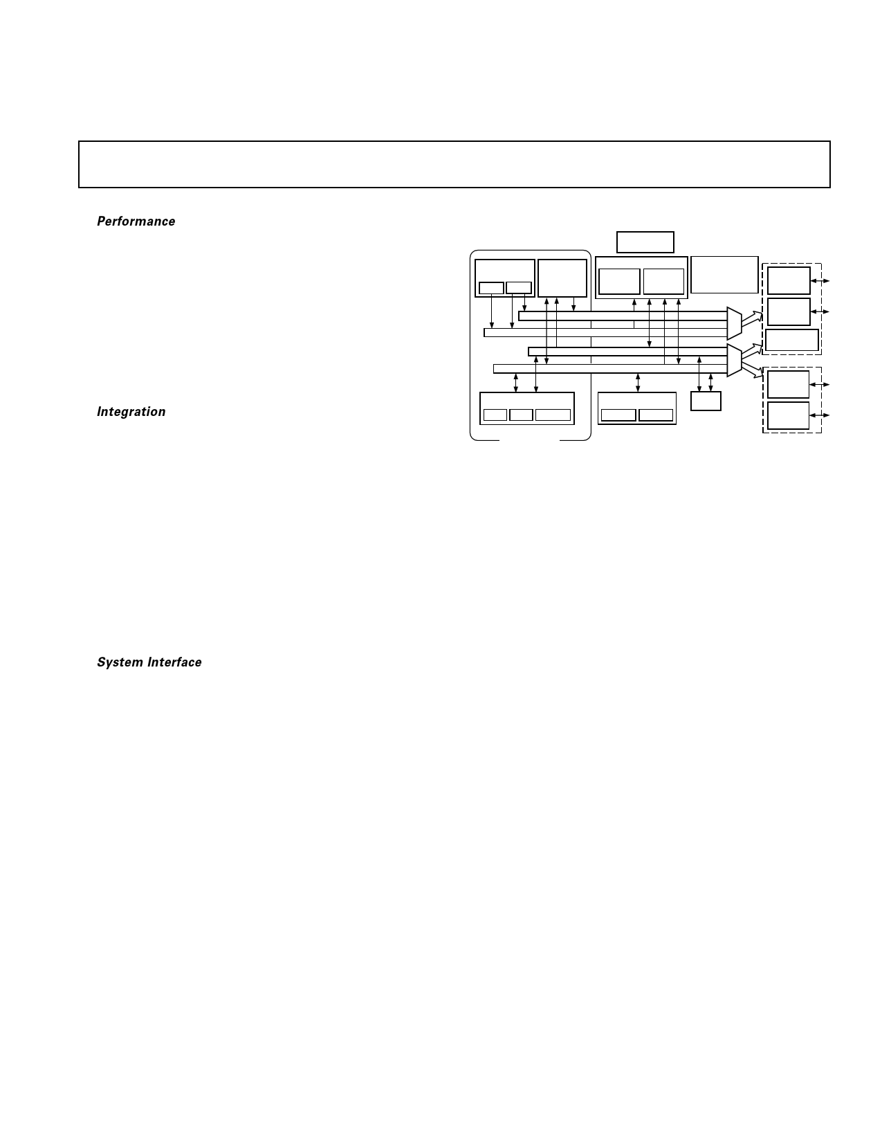
FUNCTIONAL BLOCK DIAGRAM
DATA ADDRESS
GENERATORS PROGRAM
SEQUENCER
DAG 1 DAG 2
POWER-DOWN
CONTROL
MEMORY
8K ؋ 24 8K ؋ 16
PROGRAM DATA
MEMORY MEMORY
PROGRAM MEMORY ADDRESS
DATA MEMORY ADDRESS
PROGRAM MEMORY DATA
DATA MEMORY DATA
ARITHMETIC UNITS
ALU MAC SHIFTER
ADSP-2100 BASE
ARCHITECTURE
SERIAL PORTS
SPORT 0 SPORT 1
PROGRAMMABLE
I/O
AND
FLAGS
FULL MEMORY
MODE
EXTERNAL
ADDRESS
BUS
EXTERNAL
DATA
BUS
BYTE DMA
CONTROLLER
TIMER
OR
EXTERNAL
DATA
BUS
INTERNAL
DMA
PORT
HOST MODE
13 Programmable Flag Pins Provide Flexible System
Signaling
UART Emulation through Software SPORT Reconfiguration
ICE-Port™ Emulator Interface Supports Debugging
in Final Systems
GENERAL DESCRIPTION
The ADSP-2186L is a single-chip microcomputer optimized for
digital signal processing (DSP) and other high speed numeric
processing applications.
The ADSP-2186L combines the ADSP-2100 family base archi-
tecture (three computational units, data address generators
and a program sequencer) with two serial ports, a 16-bit inter-
nal DMA port, a byte DMA port, a programmable timer, Flag
I/O, extensive interrupt capabilities and on-chip program and
data memory.
The ADSP-2186L integrates 40K bytes of on-chip memory
configured as 8K words (24-bit) of program RAM and 8K
words (16-bit) of data RAM. Power-down circuitry is also pro-
vided to meet the low power needs of battery operated portable
equipment. The ADSP-2186L is available in a 100-lead LQFP
and 144-ball mini-BGA packages.
In addition, the ADSP-2186L supports new instructions, which
include bit manipulations—bit set, bit clear, bit toggle, bit test—
new ALU constants, new multiplication instruction (x squared),
biased rounding, result free ALU operations, I/O memory trans-
fers and global interrupt masking for increased flexibility.
Fabricated in a high speed, double metal, low power, CMOS
process, the ADSP-2186L operates with a 25 ns instruction cycle
time. Every instruction can execute in a single processor cycle.
The ADSP-21xx family DSPs contain a shadow bank register
that is useful for single cycle context switching of the processor.
One Technology Way, P.O. Box 9106, Norwood, MA 02062-9106, U.S.A.
Tel: 781/329-4700 World Wide Web Site: http://www.analog.com
Fax: 781/326-8703
© Analog Devices, Inc., 2001
1 page 
ADSP-2186L
Pin Terminations (Continued)
Pin
Name
I/O
3-State
(Z)
Reset
State
Hi-Z*
Caused
By
Unused
Configuration
D4 or
IS
D3 or
IACK
D2:0 or
IAD15:13
PMS
DMS
BMS
IOMS
CMS
RD
WR
BR
BG
BGH
IRQ2/PF7
I/O (Z)
I
I/O (Z)
Hi-Z
I
Hi-Z
I/O (Z)
I/O (Z)
O (Z)
O (Z)
O (Z)
O (Z)
O (Z)
O (Z)
O (Z)
I
O (Z)
O
I/O (Z)
Hi-Z
Hi-Z
O
O
O
O
O
O
O
I
O
O
I
IRQL1/PF6 I/O (Z) I
IRQL0/PF5 I/O (Z) I
IRQE/PF4 I/O (Z) I
SCLK0
I/O
RFS0
DR0
TFS0
DT0
SCLK1
I/O
I
I/O
O
I/O
RFS1/IRQ0
DR1/FI
TFS1/IRQ1
DT1/FO
EE
EBR
EBG
ERESET
EMS
EINT
ECLK
ELIN
ELOUT
I/O
I
I/O
O
I
I
O
I
O
I
I
I
O
I
I
I
O
O
I
I
I
O
O
I
I
O
I
O
I
I
I
O
BR, EBR
BR, EBR
BR, EBR
IS
BR, EBR
BR, EBR
BR, EBR
BR, EBR
BR, EBR
BR, EBR
BR, EBR
EE
Float
High (Inactive)
Float
Float
Float
Float
Float
Float
Float
Float
Float
Float
Float
High (Inactive)
Float
Float
Input = High (Inactive)
or Program as Output,
Set to 1, Let Float
Input = High (Inactive)
or Program as Output,
Set to 1, Let Float
Input = High (Inactive)
or Program as Output,
Set to 1, Let Float
Input = High (Inactive)
or Program as Output,
Set to 1, Let Float
Input = High or Low,
Output = Float
High or Low
High or Low
High or Low
Float
Input = High or Low,
Output = Float
High or Low
High or Low
High or Low
Float
NOTES
*Hi-Z = High Impedance.
1. If the CLKOUT pin is not used, turn it OFF, using CLKODIS in Sport0
autobuffer control register.
2. If the Interrupt/Programmable Flag pins are not used, there are two options:
Option 1: When these pins are configured as INPUTS at reset and function as
interrupts and input flag pins, pull the pins High (inactive).
Option 2: Program the unused pins as OUTPUTS, set them to 1, and let
them float.
3. All bidirectional pins have three-stated outputs. When the pin is configured as
an output, the output is Hi-Z (high impedance) when inactive.
4. CLKIN, RESET, and PF3:0 are not included in the table because these pins
must be used.
Setting Memory Mode
Memory Mode selection for the ADSP-2186L is made during
chip reset through the use of the Mode C pin. This pin is multi-
plexed with the DSP’s PF2 pin, so care must be taken in how
the mode selection is made. The two methods for selecting the
value of Mode C are passive and active.
Passive configuration involves the use of a pull-up or pull-down
resistor connected to the Mode C pin. To minimize power
consumption, or if the PF2 pin is to be used as an output in the
DSP application, a weak pull-up or pull-down, on the order of
100 kΩ, can be used. This value should be sufficient to pull the
pin to the desired level and still allow the pin to operate as a
programmable flag output without undue strain on the processor’s
output driver. For minimum power consumption during
power-down, reconfigure PF2 to be an input, as the pull-up or
pull-down will hold the pin in a known state, and will not switch.
Active configuration involves the use of a three-stateable external
driver connected to the Mode C pin. A driver’s output enable
should be connected to the DSP’s RESET signal such that it
only drives the PF2 pin when RESET is active (low). After
RESET is deasserted, the driver should three-state, thus allow-
ing full use of the PF2 pin as either an input or output.
To minimize power consumption during power-down, configure
the programmable flag as an output when connected to a three-
stated buffer. This ensures that the pin will be held at a constant
level and not oscillate should the three-state driver’s level hover
around the logic switching point.
Interrupts
The interrupt controller allows the processor to respond to the
thirteen possible interrupts (eleven of which can be enabled
at any one time), and RESET with minimum overhead. The
ADSP-2186L provides four dedicated external interrupt input
pins, IRQ2, IRQL0, IRQL1 and IRQE (shared with the PF7:4
pins). In addition, SPORT1 may be reconfigured for IRQ0,
IRQ1, FI and FO, for a total of six external interrupts. The
ADSP-2186L also supports internal interrupts from the timer,
the byte DMA port, the two serial ports, software and the
power-down control circuit. The interrupt levels are internally
prioritized and individually maskable (except power-down and
RESET). The IRQ2, IRQ0 and IRQ1 input pins can be pro-
grammed to be either level- or edge-sensitive. IRQL0 and
IRQL1 are level-sensitive and IRQE is edge-sensitive. The priori-
ties and vector addresses of all interrupts are shown in Table I.
Table I. Interrupt Priority and Interrupt Vector Addresses
Source Of Interrupt
Interrupt Vector Address (Hex)
RESET (or Power-Up with
PUCR = 1)
Power-Down (Nonmaskable)
IRQ2
IRQL1
IRQL0
SPORT0 Transmit
SPORT0 Receive
IRQE
BDMA Interrupt
SPORT1 Transmit or IRQ1
SPORT1 Receive or IRQ0
Timer
0000 (Highest Priority)
002C
0004
0008
000C
0010
0014
0018
001C
0020
0024
0028 (Lowest Priority)
REV. B
–5–
5 Page 
ADSP-2186L
Table VI. Boot Summary Table
Mode C
0
Mode B
0
Mode A
0
Booting Method
BDMA feature is used to load
the first 32 program memory
words from the byte memory
space. Program execution is
held off until all 32 words
have been loaded. Chip is
configured in Full Memory
Mode.
0 1 0 No Automatic boot opera-
tions occur. Program execu-
tion starts at external memory
location 0. Chip is config-
ured in Full Memory Mode.
BDMA can still be used but
the processor does not auto-
matically use or wait for these
operations.
1 0 0 BDMA feature is used to load
the first 32 program memory
words from the byte memory
space. Program execution is
held off until all 32 words
have been loaded. Chip is
configured in Host Mode.
Additional interface hardware
is required.
1 0 1 IDMA feature is used to
load any internal memory as
desired. Program execution is
held off until internal program
memory location 0 is written
to. Chip is configured in
Host Mode.
IDMA Booting
The ADSP-2186L can also boot programs through its Internal
DMA port. If Mode C = 1, Mode B = 0, and Mode A = 1, the
ADSP-2186L boots from the IDMA port. The IDMA feature
can load as much on-chip memory as desired. Program execu-
tion is held off until on-chip program memory location 0 is
written to.
Bus Request and Bus Grant
The ADSP-2186L can relinquish control of the data and address
buses to an external device. When the external device requires
access to memory, it asserts the bus request (BR) signal. If the
ADSP-2186L is not performing an external memory access, it
responds to the active BR input in the following processor cycle by:
• Three-stating the data and address buses and the PMS, DMS,
BMS, CMS, IOMS, RD, WR output drivers,
• Asserting the bus grant (BG) signal, and
• Halting program execution.
If Go Mode is enabled, the ADSP-2186L will not halt program
execution until it encounters an instruction that requires an
external memory access.
If the ADSP-2186L is performing an external memory access
when the external device asserts the BR signal, it will not three-
state the memory interfaces or assert the BG signal until the
processor cycle after the access completes. The instruction does
not need to be completed when the bus is granted. If a single
instruction requires two external memory accesses, the bus will
be granted between the two accesses.
When the BR signal is released, the processor releases the BG
signal, reenables the output drivers and continues program
execution from the point at which it stopped.
The bus request feature operates at all times, including when
the processor is booting and when RESET is active.
The BGH pin is asserted when the ADSP-2186L is ready to
execute an instruction but is stopped because the external bus is
already granted to another device. The other device can release
the bus by deasserting bus request. Once the bus is released, the
ADSP-2186L deasserts BG and BGH and executes the external
memory access.
Flag I/O Pins
The ADSP-2186L has eight general purpose programmable input/
output flag pins. They are controlled by two memory mapped
registers. The PFTYPE register determines the direction,
1 = output and 0 = input. The PFDATA register is used to read
and write the values on the pins. Data being read from a pin
configured as an input is synchronized to the ADSP-2186L’s
clock. Bits that are programmed as outputs will read the value
being output. The PF pins default to input during reset.
In addition to the programmable flags, the ADSP-2186L has
five fixed-mode flags, FI, FO, FL0, FL1, and FL2. FL0-FL2
are dedicated output flags. FI and FO are available as an
alternate configuration of SPORT1.
Note: Pins PF0, PF1 and PF2 are also used for device configu-
ration during reset.
BIASED ROUNDING
A mode is available on the ADSP-2186 or ADSP-2186L to allow
biased rounding in addition to the normal unbiased rounding.
When the BIASRND bit is set to 0, the normal unbiased round-
ing operations occur. When the BIASRND bit is set to 1, biased
rounding occurs instead of the normal unbiased rounding. When
operating in biased rounding mode all rounding operations with
MR0 set to 0x8000 will round up, rather than only rounding up
odd MR1 values.
For example:
Table VII. Biased Rounding Example
MR Value
Before RND
00-0000-8000
00-0001-8000
00-0000-8001
00-0001-8001
00-0000-7FFF
00-0001-7FFF
Biased
RND Result
00-0001-8000
00-0002-8000
00-0001-8001
00-0002-8001
00-0000-7FFF
00-0001-7FFF
Unbiased
RND Result
00-0000-8000
00-0002-8000
00-0001-8001
00-0002-8001
00-0000-7FFF
00-0001-7FFF
REV. B
–11–
11 Page | ||
| Páginas | Total 30 Páginas | |
| PDF Descargar | [ Datasheet ADSP-2186L.PDF ] | |
Hoja de datos destacado
| Número de pieza | Descripción | Fabricantes |
| ADSP-2186 | DSP Microcomputer | Analog Devices |
| ADSP-2186 | DSP Microcomputer | Analog Devices |
| ADSP-2186BCA-160 | DSP Microcomputer | Analog Devices |
| ADSP-2186BST-115 | DSP Microcomputer | Analog Devices |
| Número de pieza | Descripción | Fabricantes |
| SLA6805M | High Voltage 3 phase Motor Driver IC. |
Sanken |
| SDC1742 | 12- and 14-Bit Hybrid Synchro / Resolver-to-Digital Converters. |
Analog Devices |
|
DataSheet.es es una pagina web que funciona como un repositorio de manuales o hoja de datos de muchos de los productos más populares, |
| DataSheet.es | 2020 | Privacy Policy | Contacto | Buscar |