|
|
|
PDF ADSP-2141L Data sheet ( Hoja de datos )
| Número de pieza | ADSP-2141L | |
| Descripción | DSP | |
| Fabricantes | Analog Devices | |
| Logotipo | ||
Hay una vista previa y un enlace de descarga de ADSP-2141L (archivo pdf) en la parte inferior de esta página. Total 30 Páginas | ||
|
No Preview Available !
a
R
DSP
ADSP-2141L
APPLICATIONS
Security Coprocessor for High Speed Networking Prod-
ucts (Routers, Switches, Hubs)
Cryptographic Core for Firewalls, Hardware Encryptors,
and More
Crypto Peripheral for Implementing Secure NIC Adapt-
ers (10/100 Ethernet, Token Ring, ISDN)
Secure Modem-on-a-Chip (V.34, ADSL)
FEATURES
DES CRYPTO BLOCK
640 Mbps Sustained Performance—Single DES
214 Mbps Sustained Performance—Triple DES
Supports All Modes: ECB; CBC; 64-Bit OFB; and 1-, 8-,
64-Bit CFB. Includes Automatic Padding
Implements IPsec ESP Transforms Autonomously at
OC-3 (155 Mbps) Rates (3-DES, SHA-1)
HASH BLOCK
Hardware-Based SHA-1 and MD-5 Hashing
253 Mbps Sustained Performance—SHA-1
315 Mbps Sustained Performance—MD-5
Implements IPsec AH and HMAC Transforms
SECURE KERNEL CONTROL
Tamper-Resistant Isolation of Cryptographic Functions
Enforces Security Perimeter Around Crypto Functions
and Crypto Storage Locations
Anticloning Protection
Secure Algorithm Download
SafeNet CGX LIBRARY
On-Chip SafeNet CGX Crypto Library with Flexible CGX
API
Includes Chained and Parallel Execution Commands
Such as Hash-and-Encrypt
Embodied as 32K Words (32K ؋ 24) Kernel Program
Mask-Programmed into On-Chip ROM
On-Chip Protected 4K ؋ 16 Security Scratchpad RAM
RANDOM NUMBER GENERATOR
Hardware-Based Nondeterministic Random Number
Generator
Generates Internal Session Keys That Are Never
Exposed Outside of the SafeNet DSP
Redundant Fail-Safe Design
Up to 1.3 Mbits of Random Data Available per Second
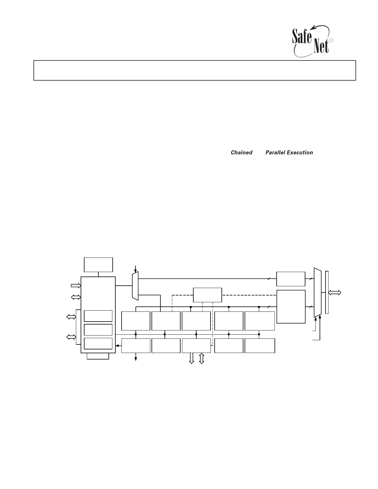
FUNCTIONAL BLOCK DIAGRAM
INTERRUPTS
FLAGS
SPORT 0
SERIAL
PORTS
SPORT 1
KERNEL
MODE
CONTROL
ADSP-218x
DSP CORE
KERNEL ROM
32K ؋ 24
PROG ROM
16K ؋ 24
DATA ROM
16K ؋ 16
TIMER
BUS_MODE
IDMA
BUS
IDMA MODE
PCI MODE
DMA-32
CONTROLLER
PROTECTED
KERNEL
RAM
(4K ؋ 16)
ENCRYPT
BLOCK
(DES, 3-DES)
HASH
BLOCK
(MD-5, SHA-1)
RNG
BLOCK
INTERRUPT APPLICATION
CONTROLLER REGISTERS
EXTERNAL
MEMORY
INTERFACE
LASER
VARIABLE
STORE
PF7/ INT_H
26-BITS
ADDR
32-BITS
DATA
RAM/ROM
16
IDMA
16
INTERFACE
32
PCI OR
32
CARDBUS
INTERFACE
PUBLIC KEY
ACCELERATOR
EMI BUS
SERIAL
EEPROM
INTERFACE
BUS_MODE
BUS_SEL
16-
OR
32-BIT
BUS
SafeNet is a registered trademark of Information Resource Engineering (IRE).
REV. 0
Information furnished by Analog Devices is believed to be accurate and
reliable. However, no responsibility is assumed by Analog Devices for its
use, nor for any infringements of patents or other rights of third parties
which may result from its use. No license is granted by implication or
otherwise under any patent or patent rights of Analog Devices.
One Technology Way, P.O. Box 9106, Norwood, MA 02062-9106, U.S.A.
Tel: 781/329-4700 World Wide Web Site: http://www.analog.com
Fax: 781/326-8703
© Analog Devices, Inc., 2000
1 page 
• IRQ2 now can include interrupt sources from the crypto
subsystem, depending on interrupt mask registers.
• A new read register has been added to indicate the state of
interrupt enable and interrupt masks.
• The kernel mode control subsystem has been added to super-
vise the protected mode of operation of the DSP core.
• Internal RAM protection logic has been added to allow the
kernel to seize increments of 1K word of internal PRAM and
DRAM.
• Bus mode configuration (218x vs. PCI) pins have been added.
• 32K words of kernel program ROM have been added to the
DSP memory space. (See the Memory Map section.)
Kernel Mode Control
The kernel mode control subsystem provides the following
functions which serve to enforce the security integrity of the
ADSP-2141L:
• Provide a means to securely enter the kernel mode.
• Provide a means to properly exit the kernel mode.
• Prevent user mode access to protected memory and register
locations.
• Manage interrupts during kernel mode executions.
• Manage the reset function to ensure that sensitive variables
in DSP registers are erased.
Most of the kernel mode control functions are implemented in
the hardware of the ADSP-2141L and are not directly visible to
nonkernel applications (user mode). Any attempt by a user
mode application program running on the DSP to access a
kernel space addresses (PRAM 0x2001 – 0x3FFF, PMOVLAY
000C – 000F; or DRAM 0x0000 – 0x17FF, DMOVLAY 000F)
results in an immediate chip reset and all sensitive registers and
memory locations are erased. Kernel mode may only be entered
via a call, jump or increment to address 0x2000 with PMOVLAY
REGISTER
ADDRESS
7
WR
ADSP-2141L
set to 0x000F. Once in kernel mode, any branch to nonkernel
space program memory causes the DSP to return to user mode.
(Note: For security reasons when in kernel mode, the DSP does
not respond to Emulator bus requests.)
The kernel mode can be interrupted during execution; however,
during certain periods where sensitive data is being moved, all
interrupts are disabled. Within the interrupt service routine,
another call to the kernel (CGX call) may be made if desired,
although there are limitations on which CGX commands may
preempt another. (For information, see the ADSP-2141L CGX
Interface Programmer’s Guide http://www.ire-ma.com/proddoc.htm.)
Only one level of kernel mode nesting is permitted. An interrupt
to a user mode vector location while in nested kernel mode will
also trigger the violation reset logic.
Once the interrupt service routine is finished, the return-from-
interrupt must return control back to the kernel at the address/
overlay that was originally interrupted, otherwise the protection
logic will issue a chip reset.
Hash and Encrypt Block Overview
The encrypt block is tightly coupled to the hash block in the
ADSP-2141L and therefore the two are discussed together.
Refer to Figure 4, Hash/Encrypt Functional Block Diagram, for
the following description.
The algorithms implemented in the combined hash and encryp-
tion block are: DES, Triple DES, MD-5 and SHA-1. Data can
be transferred to and from the module once to perform both
hashing and encryption on the same data stream. The DES
encrypt/decrypt operations are highly paralleled and pipelined,
and execute full 16-round DES in only four clock cycles. The
internal data flow and buffering allows parallel execution of
hashing and encryption where possible, and allows processing of
data concurrently with I/O of previous and subsequent blocks.
RD
DSP
OR
PCI
16-/32-BIT
INPUT
BUS
PAD
INSERTION
512-BIT
FIFO
PAD
CONSUME
AND VERIFY
ENCRYPT/
DECRYPT
BLOCK
WRITE
CONTEXT
512-BIT
FIFO
CONTEXT
STORAGE (0/1)
HASH
BLOCK
READ
CONTEXT
HASH
DIGEST
DSP
OR
PCI
16-/32-BIT
OUTPUT
BUS
REV. 0
MUTABLE BIT
PAD
PROCESSING INSERTION
(ENCRYPT-THEN-HASH)
(DECRYPT-THEN-HASH)
Figure 4. Hash/Encrypt Functional Block Diagram
–5–
5 Page 
ADSP-2141L
IDMA Mode Multiplex Bus Pin Definition
IDMA Port (218x Mode)
PIN FUNCTION DESCRIPTIONS—IDMA Mode Multiplex Bus
Pin Name
MPLX5
MPLX6
MPLX7
MPLX8
MPLX9
MPLX10
MPLX11
MPLX12
MPLX_BUS
IDMA Name
IRD
IWR
IS
IAL
IACK
FL0
FL1
FL2
IAD
Pins
1
1
1
1
1
1
1
1
16
I/O
I
I
I
I
O
O
O
O
I/O
Description
IDMA Port Read Input
IDMA Port Write Input
IDMA Port Select
IDMA Port Address Latch
IDMA Port Access Ready Acknowledge
Output Flags
Output Flags
Output Flags
IDMA Data I/O
PCI Port
Pin Name
MPLX1
MPLX2
MPLX3
MPLX4
MPLX5
MPLX6
MPLX7
MPLX8
MPLX9
MPLX10
MPLX11
MPLX12
MPLX_BUS
PF7/INT_H
PIN FUNCTION DESCRIPTIONS—PCI Mode Multiplex Bus
PCI Name
Pci_cbe3
Pci_cbe2
Pci_cbe1
Pci_cbe0
Pci_idsel
Pci_gnt
Pci_frame
Pci_devsel
Pci_trdy
Pci_perr
Pci_serr
Pci_req
Pci_ad15:0
Pci_ad31:16
Pci_intA
Pins
1
1
1
1
1
1
1
1
1
1
1
1
32
1
I/O
I/O
I/O
I/O
I/O
I
I
I/O
I/O
I/O
I/O
I/O
O
I/O
O
Description
Bus Command / Byte Enable 3
Bus Command / Byte Enable 2
Bus Command / Byte Enable 1
Bus Command / Byte Enable 0
Initialization Device Select
Bus Grant
Cycle Frame
Device Select
Target Ready
Parity Error
System Error
PCI Bus Request
PCI Address/Data Bus
PCI Interrupt A Request
SYSTEM INTERFACE
The ADSP-2141L may be integrated into a wide variety of sys-
tems, including those that already have a microprocessor and
those that will use the ADSP-2141L as the main processor. The
device can be configured into one of two Host Bus modes:
IDMA or PCI.
IDMA Bus Mode
The IDMA bus mode operates the same as in a native ADSP-
218x device, as described in this section.
The IDMA port provides an efficient means of communication
between a host system and the ADSP-2141L. The port is used
to access the on-chip program memory and data memory of the
DSP with only one DSP cycle per word overhead. The IDMA
port cannot, however, be used to write to the DSP’s memory-
mapped control registers.
The IDMA port has a 16-bit multiplexed address and data bus,
and supports reading or writing 16-bit data (DM) or 24-bit
program memory (PM). The IDMA port is completely asyn-
chronous and can be written to while the ADSP-2141L is oper-
ating at full speed.
The DSP memory address is latched and then automatically
incremented after each IDMA transaction. An external device can
therefore access a block of sequentially addressed memory by
specifying only the starting address of the block. This increases
throughput as the address does not have to be sent for each
memory access.
The IDMA port access occurs in two phases. The first is the
IDMA address latch cycle. When the acknowledge is asserted, a
14-bit address and 1-bit destination type can be driven onto the
bus by an external device. The address specifies an on-chip
memory location; the destination type specifies whether it is a
DM or PM access. The falling edge of the address latch signal
latches this value to the IDMAA register.
Once the address is stored, data can either be read from or
written to the ADSP-2141L’s on-chip memory. Asserting the
select line (IS) and the appropriate read or write line (IRD and
IWR respectively) signals the ADSP-2141L that a particular
transaction is required. In either case, there is a one-processor-
cycle delay for synchronization. The memory access consumes
an additional processor cycle.
Once an access has occurred, the latched address is automati-
cally incremented and another access can occur.
Through the IDMAA register, the ADSP-2141L can also
specify the starting address and data format for DMA operation.
Figure 6 illustrates a typical system configuration for the
IDMA mode.
REV. 0
–11–
11 Page | ||
| Páginas | Total 30 Páginas | |
| PDF Descargar | [ Datasheet ADSP-2141L.PDF ] | |
Hoja de datos destacado
| Número de pieza | Descripción | Fabricantes |
| ADSP-2141L | DSP | Analog Devices |
| ADSP-2141LKS-E1 | DSP | Analog Devices |
| ADSP-2141LKS-N1 | DSP | Analog Devices |
| Número de pieza | Descripción | Fabricantes |
| SLA6805M | High Voltage 3 phase Motor Driver IC. |
Sanken |
| SDC1742 | 12- and 14-Bit Hybrid Synchro / Resolver-to-Digital Converters. |
Analog Devices |
|
DataSheet.es es una pagina web que funciona como un repositorio de manuales o hoja de datos de muchos de los productos más populares, |
| DataSheet.es | 2020 | Privacy Policy | Contacto | Buscar |