|
|
PDF ADS8411 Data sheet ( Hoja de datos )
| Número de pieza | ADS8411 | |
| Descripción | 16-BIT/ 2 MSPS/ UNIPOLAR INPUT/ MICRO POWER SAMPLING ANALOG-TO-DIGITAL CONVERTER WITH PARALLEL INTERFACE AND REFERENCE | |
| Fabricantes | Burr-Brown Corporation | |
| Logotipo |  |
|
Hay una vista previa y un enlace de descarga de ADS8411 (archivo pdf) en la parte inferior de esta página. Total 23 Páginas | ||
|
No Preview Available !
BurrĆBrown Products
from Texas Instruments
ADS8411
SLAS369B – APRIL 2002 – REVISED DECEMBER 2004
16-BIT, 2 MSPS, UNIPOLAR INPUT, MICRO POWER SAMPLING
ANALOG-TO-DIGITAL CONVERTER WITH PARALLEL INTERFACE AND REFERENCE
FEATURES
• 2-MHz Sample Rate
• 16-Bit NMC Ensured Over Temperature
• Zero Latency
• Unipolar Single-Ended Input Range:
0 V to Vref
• Onboard Reference
• Onboard Reference Buffer
• High-Speed Parallel Interface
• Power Dissipation: 175 mW at 2 MHz Typ
• Wide Digital Supply
• 8-/16-Bit Bus Transfer
• 48-Pin TQFP Package
• ESD Sensitive – HBM Capability of 500 V,
1000 V at All Input Pins
APPLICATIONS
• DWDM
• Instrumentation
• High-Speed, High-Resolution, Zero Latency
Data Acquisition Systems
• Transducer Interface
• Medical Instruments
• Communication
DESCRIPTION
The ADS8411 is a 16-bit, 2 MHz A/D converter with
an internal 4.096-V reference. The device includes a
16-bit capacitor-based SAR A/D converter with in-
herent sample and hold. The ADS8411 offers a full
16-bit interface and an 8-bit option where data is read
using two 8-bit read cycles.
The ADS8411 has a unipolar single-ended input. It is
available in a 48-lead TQFP package and is
characterized over the industrial -40°C to 85°C tem-
perature range.
REFOUT
SAR
+IN
−IN
REFIN
+
_
CDAC
Comparator
4.096-V
Internal
Reference
Clock
Output
Latches
and
3-State
Drivers
Conversion
and
Control Logic
BYTE
16-/8-Bit
Parallel DATA
Output Bus
RESET
CONVST
BUSY
CS
RD
Please be aware that an important notice concerning availability, standard warranty, and use in critical applications of Texas
Instruments semiconductor products and disclaimers thereto appears at the end of this data sheet.
PRODUCTION DATA information is current as of publication date.
Products conform to specifications per the terms of the Texas
Instruments standard warranty. Production processing does not
necessarily include testing of all parameters.
Copyright © 2002–2004, Texas Instruments Incorporated
1 page 
ADS8411
www.ti.com
SLAS369B – APRIL 2002 – REVISED DECEMBER 2004
TIMING CHARACTERISTICS
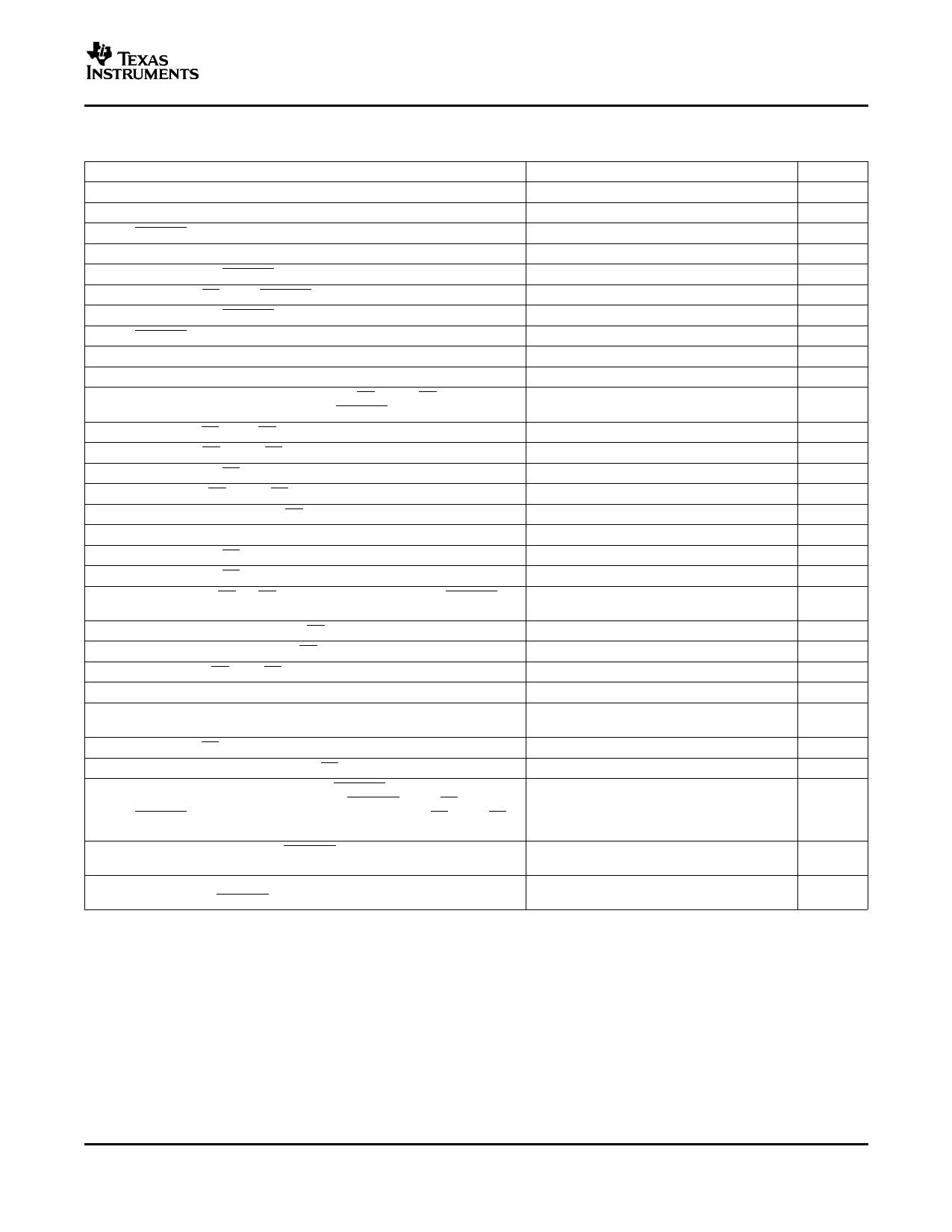
All specifications typical at –40°C to 85°C, +VA = +VBD = 5 V (1)(2)(3)
tCONV
tACQ
tpd1
tpd2
tw1
tsu1
tw2
tw3
tw4
th1
td1
tsu2
tw5
ten
td2
td3
tw6
tw7
th2
tsu3
th3
tdis
td5
tsu4
td6
td7
tsu(AB)
tsu5
th4
PARAMETER
Conversion time
Acquisition time
CONVST low to BUSY high
Propagation delay time, end of conversion to BUSY low
Pulse duration, CONVST low
Setup time, CS low to CONVST low
Pulse duration, CONVST high
CONVST falling edge jitter
Pulse duration, BUSY signal low
Pulse duration, BUSY signal high
Hold time, first data bus data transition (RD low, or CS low for read
cycle, or BYTE input changes) after CONVST low
Delay time, CS low to RD low (or BUSY low to RD low)
Setup time, RD high to CS high
Pulse duration, RD low
Enable time, RD low (or CS low for read cycle) to data valid
Delay time, data hold from RD high
Delay time, BYTE rising edge or falling edge to data valid
Pulse duration, RD high
Pulse duration, CS high
Hold time, last RD (or CS for read cycle ) rising edge to CONVST
falling edge
Setup time, BYTE transition to RD falling edge
Hold time, BYTE transition to RD falling edge
Disable time, RD high (CS high for read cycle) to 3-stated data bus
Delay time, end of conversion to MSB data valid
Byte transition setup time, from BYTE transition to next BYTE
transition
Delay time, CS rising edge to BUSY falling edge
Delay time, BUSY falling edge to CS rising edge
Setup time, from the falling edge of CONVST (used to start the valid
conversion) to the next falling edge of CONVST (when CS = 0 and
CONVST used to abort) or to the next falling edge of CS (when CS is
used to abort)
Setup time, falling edge of CONVST to read valid data (MSB) from
current conversion
Hold time, data (MSB) from previous conversion hold valid from
falling edge of CONVST
MIN
340
100
20
0
20
Min(tACQ)
40
0
0
50
0
2
20
20
50
0
0
50
50
50
60
MAX(tCONV) + MAX(td5)
TYP MAX
400
30
5
10
370
20
20
20
10
340
MIN(tCONV)
UNIT
ns
ns
ns
ns
ns
ns
ns
ps
ns
ns
ns
ns
ns
ns
ns
ns
ns
ns
ns
ns
ns
ns
ns
ns
ns
ns
ns
ns
ns
ns
(1) All input signals are specified with tr = tf = 5 ns (10% to 90% of +VBD) and timed from a voltage level of (VIL + VIH)/2.
(2) See timing diagrams.
(3) All timings are measured with 20 pF equivalent loads on all data bits and BUSY pins.
5
5 Page 
www.ti.com
TIMING DIAGRAMS (continued)
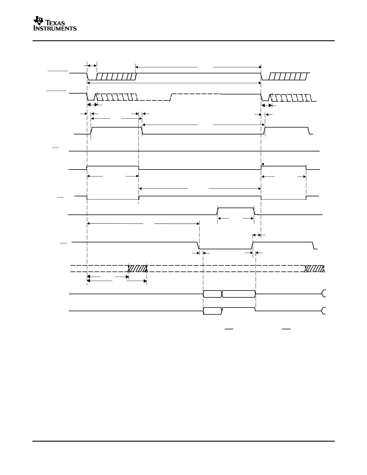
tw1
CONVST
(used in normal
conversion)
CONVST
(used in ABORT)
tpd1
BUSY
tsu(AB)
tw4
tpd2
ADS8411
SLAS369B – APRIL 2002 – REVISED DECEMBER 2004
tw2
tcycle
tsu(AB)
tpd1
tw3
CS = 0
CONVERT†
SAMPLING†
(When CS = 0)
BYTE
tCONV
th1
t(ACQ)
tsu4
RD
Data to
be read†
DB[15:8]
Invalid
Previous Conversion
th4
tsu5
Hi−Z
ten
Current Conversion
D [15:8]
D [7:0]
tCONV
th2
tdis
Invalid
Hi−Z
DB[7:0]
Hi−Z
D [7:0]
Hi−Z
†Signal internal to device
Figure 3. Timing for Conversion and Acquisition Cycles With CS Tied to BDGND, RD Toggling
11
11 Page | ||
| Páginas | Total 23 Páginas | |
| PDF Descargar | [ Datasheet ADS8411.PDF ] | |
Hoja de datos destacado
| Número de pieza | Descripción | Fabricantes |
| ADS8410 | 16-Bit 2-MSPS LVDS Serial Interface SAR ADC. (Rev. A) | Texas Instruments |
| ADS8411 | 16-BIT/ 2 MSPS/ UNIPOLAR INPUT/ MICRO POWER SAMPLING ANALOG-TO-DIGITAL CONVERTER WITH PARALLEL INTERFACE AND REFERENCE | Burr-Brown Corporation |
| ADS8411 | 16-BIT/ 2 MSPS/ UNIPOLAR INPUT/ MICRO POWER SAMPLING ANALOG-TO-DIGITAL CONVERTER WITH PARALLEL INTERFACE AND REFERENCE | Burr-Brown Corporation |
| ADS8411 | 16-Bit 2 MSPS Unipolar Input Micropower Sampling Analog to Digital Converter (Rev. B) | Texas Instruments |
| Número de pieza | Descripción | Fabricantes |
| SLA6805M | High Voltage 3 phase Motor Driver IC. |
Sanken |
| SDC1742 | 12- and 14-Bit Hybrid Synchro / Resolver-to-Digital Converters. |
Analog Devices |
|
DataSheet.es es una pagina web que funciona como un repositorio de manuales o hoja de datos de muchos de los productos más populares, |
| DataSheet.es | 2020 | Privacy Policy | Contacto | Buscar |
