|
|
PDF ADS830E Data sheet ( Hoja de datos )
| Número de pieza | ADS830E | |
| Descripción | 8-Bit/ 60MHz Sampling ANALOG-TO-DIGITAL CONVERTER | |
| Fabricantes | Burr-Brown Corporation | |
| Logotipo |  |
|
Hay una vista previa y un enlace de descarga de ADS830E (archivo pdf) en la parte inferior de esta página. Total 11 Páginas | ||
|
No Preview Available !
®
ADS830 ¤
ADS830
TM 8-Bit, 60MHz Sampling
ANALOG-TO-DIGITAL CONVERTER
FEATURES
q HIGH SNR: 49.5dB
q INTERNAL /EXTERNAL REFERENCE
OPTION
q SINGLE-ENDED OR
DIFFERENTIAL ANALOG INPUT
q PROGRAMMABLE INPUT RANGE:
1Vp-p /2Vp-p
q LOW POWER: 170mW
q LOW DNL: 0.2LSB
q SINGLE +5V SUPPLY OPERATION
q 20-PIN SSOP PACKAGE
APPLICATIONS
q MEDICAL IMAGING
q VIDEO DIGITIZING
q COMMUNICATIONS
q DISK-DRIVE CONTROL
DESCRIPTION
The ADS830 is a pipeline, CMOS analog-to-digital con-
verter that operates from a single +5V power supply. This
converter provides excellent performance with a single-
ended input and can be operated with a differential input
for added spurious performance. This high performance
converter includes an 8-bit quantizer, high bandwidth
track/hold, and a high accuracy internal reference. It also
allows for the user to disable the internal reference and
utilize external references. This external reference option
provides excellent gain and offset matching when used in
multi-channel applications or in applications where DC full
scale range adjustment is required.
The ADS830 employs digital error correction techniques to
provide excellent differential linearity for demanding im-
aging applications. Its low distortion and high SNR give
the extra margin needed for medical imaging, communica-
tions, video, and test instrumentation.
The ADS830 is specified at a maximum sampling fre-
quency of 60MHz and a single-ended input range of 1.5V
to 3.5V. The ADS830 is available in a 20-lead SSOP
package and is pin-for-pin compatible with the 8-bit, 80MHz
ADS831.
+VS
ADS830
CLK
Timing
Circuitry
VDRV
VIN IN
IN
(Opt)
T/H
8-Bit
Pipelined
A/D Core
Error
Correction
Logic
3-State
Outputs
D0
•••
D7
Internal
Reference
Optional External Int/Ext
Reference
International Airport Industrial Park • Mailing Address: PO Box 11400, Tucson, AZ 85734 • Street Address: 6730 S. Tucson Blvd., Tucson, AZ 85706 • Tel: (520) 746-1111
Twx: 910-952-1111 • Internet: http://www.burr-brown.com/ • Cable: BBRCORP • Telex: 066-6491 • FAX: (520) 889-1510 • Immediate Product Info: (800) 548-6132
©1998 Burr-Brown Corporation
PDS-1429B
Printed in U.S.A. October, 1998
1 page 
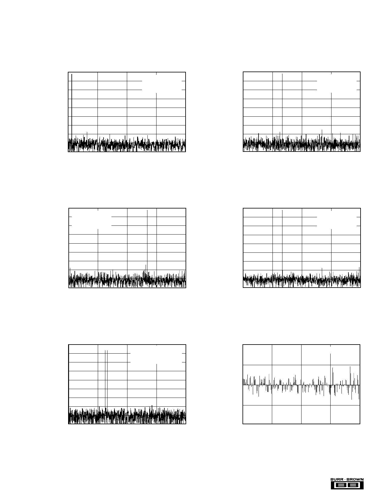
TYPICAL PERFORMANCE CURVES
At TA = full specified temperature range, single-ended input range = 1.5V to 3.5V, sampling rate = 60MHz, and external reference, unless otherwise noted.
0
–10
–20
–30
–40
–50
–60
–70
–80
–90
0
SPECTRAL PERFORMANCE
fIN = 1MHz
SNR = 49dBFS
SFDR = 67dBFS
7.5 15 22.5
Frequency (MHz)
30
0
–10
–20
–30
–40
–50
–60
–70
–80
–90
0
SPECTRAL PERFORMANCE
fIN = 10MHz
SNR = 49dBFS
SFDR = 65dBFS
7.5 15 22.5
Frequency (MHz)
30
SPECTRAL PERFORMANCE
0
–10
fIN = 20MHz
SNR = 49dBFS
–20 SFDR = 63dBFS
–30
–40
–50
–60
–70
–80
–90
0
7.5 15 22.5
Frequency (MHz)
30
0
–10
–20
–30
–40
–50
–60
–70
–80
–90
0
SPECTRAL PERFORMANCE
(Single-Ended, 1Vp-p)
fIN = 10MHz
SNR = 49dBFS
SFDR = 65dBFS
7.5 15 22.5
Frequency (MHz)
30
0
–10
–20
–30
–40
–50
–60
–70
–80
–90
0
TWO-TONE INTERMODULATION DISTORTION
f1 = 9.5MHz at –7dBFS
f2 = 9.9MHz at –7dBFS
IMD(3) = –60dBc
7.5 15 22.5
Frequency (MHz)
30
0.2
0.1
0
–0.1
–0.2
0
DIFFERENTIAL LINEARITY ERROR
fIN = 10MHz
64 128 192
Output Code
256
®
5 ADS830
5 Page 
lower CMV as it increases the signal headroom of the
driving amplifier. The internal reference ladder has a nomi-
nal impedance of 800Ω. Depending on the selected refer-
ence voltages, the required drive current will vary accord-
ingly and the external reference circuitry should be designed
to supply the maximum required current.
DIGITAL INPUTS AND OUTPUTS
Clock Input Requirements
Clock jitter is critical to the SNR performance of high speed,
high resolution Analog to Digital Converters. It leads to
aperture jitter (tA) which adds noise to the signal being
converted. The ADS830 samples the input signal on the
Digital Output Driver (VDRV)
The ADS830 features a dedicated supply pin for the output
logic drivers, VDRV, which is not internally connected to
the other supply pins. Setting the voltage at VDRV to +5V
or +3V, the ADS830 produces corresponding logic levels
and can directly interface to the selected logic family. The
output stages are designed to supply sufficient current to
drive a variety of logic families. However, it is recom-
mended to use the ADS830 with +3V logic supply. This will
lower the power dissipation in the output stages due to the
lower output swing and reduce current glitches on the supply
line which may affect the ac performance of the converter.
In some applications, it might be advantageous to decouple
the VDRV pin with additional capacitors or a pi-filter.
rising edge of the CLK input. Therefore, this edge should
have the lowest possible jitter. The jitter noise contribution
to total SNR is given by the following equation. If this value
is near your system requirements, input clock jitter must be
reduced.
Jitter SNR = 20 log 1
rms signal to rms noise
2πƒIN t A
Where: ƒIN is Input Signal Frequency
tA is rms Clock Jitter
Particularly in udersampling applications, special consider-
ation should be given to clock jitter. The clock input should
be treated as an analog input in order to achieve the highest
level of performance. Any overshoot or undershoot of the
clock signal may cause degradation of the performance.
When digitizing at high sampling rates, the clock should
have a 50% duty cycle (tH = tL), along with fast rise and fall
times of 2ns or less.
Digital Outputs
The output data format of the ADS830 is in positive Straight
Offset Binary code, see Table I. This format can easily
converted into the Two’s Binary Complement code by
inverting the MSB.
SINGLE-ENDED INPUT (2Vp-p)
(IN = CMV)
+FS (IN = +3.5V)
+1/2 FS
+1LSB
Bipolar Zero (IN = 2.5V)
–1LSB
–1/2 FS
–FS (IN = +1.5V)
STRAIGHT OFFSET BINARY
(SOB)
1111 1111
1100 0000
1000 0001
1000 0000
0111 1111
0100 0000
0000 0000
GROUNDING AND DECOUPLING
Proper grounding and bypassing, short lead length, and the
use of ground planes are particularly important for high
frequency designs. Multilayer PC boards are recommended
for best performance since they offer distinct advantages
like minimizing ground impedance, separation of signal
layers by ground layers, etc. The ADS830 should be treated
as an analog component. Whenever possible, the supply pins
should be powered by the analog supply. This will ensure
the most consistent results, since digital supply lines often
carry high levels of noise which otherwise would be coupled
into the converter and degrade the achievable performance.
All ground connections on the ADS830 are internally joined
together, obviating the design of split ground planes. The
ground pins (1, 18) should directly connect to an analog
ground plane which covers the PC board area around the
converter. While designing the layout, it is important to keep
the analog signal traces separated from any digital lines to
prevent noise coupling onto the analog signal path. Because
of its high sampling rate, the ADS830 generates high fre-
quency current transients and noise (clock feedthrough) that
are fed back into the supply and reference lines. This
requires that all supply and reference pins are sufficiently
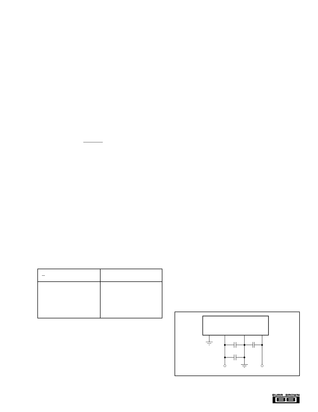
bypassed. Figure 9 shows the recommended decoupling
scheme for the ADS830. In most cases 0.1µF ceramic chip
capacitors at each pin are adequate to keep the impedance
low over a wide frequency range. Their effectiveness largely
depends on the proximity to the individual supply pin.
Therefore, they should be located as close to the supply pins
as possible. In addition, a larger bipolar capacitor (1µF to
22µF) should be placed on the PC board in proximity of the
converter circuit.
TABLE I. Coding Table for the ADS830.
It is recommended to keep the capacitive loading on the data
lines as low as possible (≤ 15pF). Higher capacitive loading
will cause larger dynamic currents as the digital outputs are
changing. Those high current surges can feed back to the
analog portion of the ADS830 and affect the performance. If
necessary, external buffers or latches close to the converter’s
output pins may be used to minimize the capacitive loading.
They also provide the added benefit of isolating the ADS830
from any digital noise activities on the bus coupling back
high frequency noise.
GND
1
ADS830
+VS GND VDRV
19 18 20
0.1µF 0.1µF
10µF
+
+5V +3/+5V
FIGURE 9. Recommended Bypassing for the Supply Pins.
®
11 ADS830
11 Page | ||
| Páginas | Total 11 Páginas | |
| PDF Descargar | [ Datasheet ADS830E.PDF ] | |
Hoja de datos destacado
| Número de pieza | Descripción | Fabricantes |
| ADS830 | 8-Bit/ 60MHz Sampling ANALOG-TO-DIGITAL CONVERTER | Burr-Brown Corporation |
| ADS830 | ADS830: SpeedPlus 8-Bit 60MHz Sampling Analog-To-Digital Converter (Rev. A) | Texas Instruments |
| ADS830E | 8-Bit/ 60MHz Sampling ANALOG-TO-DIGITAL CONVERTER | Burr-Brown Corporation |
| Número de pieza | Descripción | Fabricantes |
| SLA6805M | High Voltage 3 phase Motor Driver IC. |
Sanken |
| SDC1742 | 12- and 14-Bit Hybrid Synchro / Resolver-to-Digital Converters. |
Analog Devices |
|
DataSheet.es es una pagina web que funciona como un repositorio de manuales o hoja de datos de muchos de los productos más populares, |
| DataSheet.es | 2020 | Privacy Policy | Contacto | Buscar |
