|
|
|
PDF ADS2806 Data sheet ( Hoja de datos )
| Número de pieza | ADS2806 | |
| Descripción | Dual/ 12-Bit/ 32MHz Sampling ANALOG-TO-DIGITAL CONVERTER | |
| Fabricantes | Burr-Brown Corporation | |
| Logotipo | ||
Hay una vista previa y un enlace de descarga de ADS2806 (archivo pdf) en la parte inferior de esta página. Total 19 Páginas | ||
|
No Preview Available !
ADS2806
ADS2806
SBAS178B – DECEMBER 2000 – REVISED MAY 2002
Dual, 12-Bit, 32MHz Sampling
ANALOG-TO-DIGITAL CONVERTER
FEATURES
q SPURIOUS-FREE DYNAMIC RANGE:
73dB at 10MHz fIN
q HIGH SNR: 67dB (2Vp-p), 69dB (3Vp-p)
q INTERNAL OR EXTERNAL REFERENCE
q LOW DLE: ±0.4LSB
q FLEXIBLE INPUT RANGE: 2Vp-p to 3Vp-p
q TQFP-64 POWER PACKAGE
DESCRIPTION
The ADS2806 is a dual, high-speed, high dynamic range,
12-bit pipelined Analog-to-Digital Converter (ADC). This con-
verter includes a high-bandwidth track-and-hold that gives
excellent spurious performance up to and beyond the Nyquist
rate. The differential nature of this track-and-hold and ADC
circuitry minimizes even-order harmonics and gives excel-
lent common-mode noise immunity. The track-and-hold can
also be operated single-ended.
The ADS2806 provides for setting the full-scale range of the
converter without any external reference circuitry. The internal
+VS
APPLICATIONS
q COMMUNICATIONS IF PROCESSING
q COMMUNICATIONS BASESTATIONS
q TEST EQUIPMENT
q MEDICAL IMAGING
q VIDEO DIGITIZING
q CCD DIGITIZING
reference can be disabled allowing low drive, external refer-
ences to be used for improved tracking in multichannel systems.
The ADS2806 provides an over-range indicator flag to
indicate an input signal that exceeds the full-scale input
range of the converter. This flag can be used to reduce the
gain of front end gain control circuitry. There is also an
output enable pin to allow for multiplexing and testability on
a PC board.
The ADS2806 employs digital error correction techniques to
provide excellent differential linearity for demanding imag-
ing applications. The ADS2806 is available in a TQFP-64
power package.
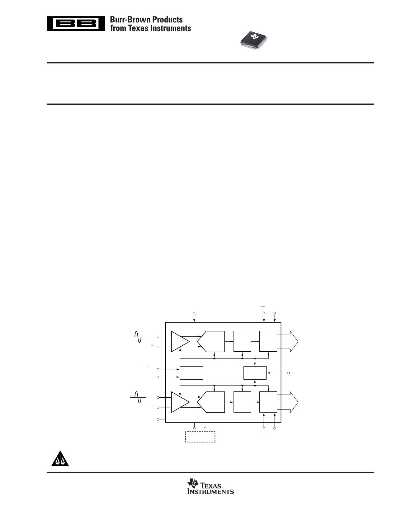
OEA OVRA
ADS2806
VIN INA
T&H
INA
(Opt.)
12-Bit
Pipelined
A/D
Error
Correction
Logic
3-State
Outputs
D12A
•
•
•
D1A
INT/EXT
FSSEL
Internal
Reference
Timing
Circuitry
CLK
VIN INB
T&H
INB
(Opt.)
CM
12-Bit
Pipelined
A/D
Error
Correction
Logic
3-State
Outputs
D12B
•
•
•
D1B
Optional External
Reference
OEB OVRB
Please be aware that an important notice concerning availability, standard warranty, and use in critical applications of
Texas Instruments semiconductor products and disclaimers thereto appears at the end of this data sheet.
PRODUCTION DATA information is current as of publication date.
Products conform to specifications per the terms of Texas Instruments
standard warranty. Production processing does not necessarily include
testing of all parameters.
www.ti.com
Copyright © 2000, Texas Instruments Incorporated
1 page 
PIN DESCRIPTIONS
PIN I/O DESIGNATOR DESCRIPTION
1
GND
Ground
2
GND
Ground
3 +VS +5V Supply
4
GND
Ground
5 +VS +5V Supply
6 I OEB Output Enable, Channel B
7
GND
GND
8
VDRVB
Logic Driver Supply Voltage, Channel B
9 O OVRB Over-Range Indicator, Channel B
10 O B12 (LSB) Data Bit 12 (D0), Channel B
11 O
B11 Data Bit 11 (D1), Channel B
12 O B10 Data Bit 10 (D2), Channel B
13 O B9 Data Bit 9 (D3), Channel B
14 O B8 Data Bit 8 (D4), Channel B
15 O B7 Data Bit 7 (D5), Channel B
16 O B6 Data Bit 6 (D6), Channel B
17 O B5 Data Bit 5 (D7), Channel B
18 O B4 Data Bit 4 (D8), Channel B
19 O B3 Data Bit 3 (D9), Channel B
20 O B2 Data Bit 2 (D10), Channel B
21 O B1 (MSB) Data Bit 1 (D11), Channel B
22 O
23
DVB
GND
Data Valid, Channel B
Ground
24 I
CLK
Clock
25
GND
Ground
26 O DVA Data Valid, Channel A
27 O A12 (LSB) Data Bit 12 (D0), Channel A
28 O A11 Data Bit 11 (D1), Channel A
29 O A10 Data Bit 10 (D2), Channel A
30 O A9 Data Bit 9 (D3), Channel A
31 O A8 Data Bit 8 (D4), Channel A
32 O A7 Data Bit 7 (D5), Channel A
33 O A6 Data Bit 6 (D6), Channel A
PIN I/O DESIGNATOR DESCRIPTION
34 O A5 Data Bit 5 (D7), Channel A
35 O A4 Data Bit 4 (D8), Channel A
36 O A3 Data Bit 3 (D9), Channel A
37 O A2 Data Bit 2 (D10), Channel A
38 O A1 (MSB) Data Bit 1 (D11), Channel A
39 O
OVRA
Over-Range Indicator, Channel A
40
VDRVA
Logic Driver Supply Voltage, Channel A
41
GND
Ground
42 I
43
44
OEA
+VS
GND
Output Enable, Channel A
+5V Supply
Ground
45 I
SEL Input Range Select: HIGH = 3V, LOW = 2V
46 +VS +5V Supply
47
GND
Ground
48
GND
Ground
49
GND
Ground
50 I
51 I
52 O
53 I/O
54 I/O
55
INA
INA
CMA
REFTA
REFBA
GND
Analog Input, Channel A
Complementary Analog Input, Channel A
Common-Mode, Channel A
Top Reference/Bypass, Channel A
Bottom Reference/Bypass, Channel A
Ground
56 I INT/EXT Reference Select: HIGH = External,
LOW = Internal 50kΩ Pull-Up Resistor
57 +VS +5V Supply
58
GND
Ground
59 I/O
60 I/O
61 O
62 I
63 I
64
REFBB
REFTB
CMB
INB
INB
GND
Bottom Reference/Bypass, Channel B
Top Reference/Bypass, Channel B
Common-Mode, Channel B
Complementary Analog Input, Channel B
Analog Input, Channel B
Ground
ADS2806
SBAS178B
www.ti.com
5
5 Page 
Figure 2 shows an example of such an interface circuit
specifically designed to maximize the dynamic performance.
The voltage feedback amplifier, OPA642, maintains an
excellent distortion performance for input frequencies of up
to 15MHz. The two amplifiers (A1, A2) are configured as an
inverting and noninverting gain stage to convert the input
signal from single-ended to differential. The nominal gain for
this stage is set to +2V/V. The outputs of the OPA642s are
AC-coupled to the converter’s differential inputs. This will
keep the distortion performance at its best since the signal
range stays within the linear region of the op amp and
sufficient headroom to the supply rails can be maintained.
Four resistors located between the top (REFT) and bottom
(REFB) reference shift the input signal to a common-mode
voltage of approximately +2.5V.
The interface circuit of Figure 2 can be modified to extend
the bandwidth to approximately 25MHz, by replacing the
OPA642 with its decompensated version, the OPA643. The
OPA643 provides the necessary slew rate for a low distor-
tion front end to the ADS2806. With a minimum gain stability
of +3, the gain resistors have to be modified, as well as
optimizing the series resistor and shunt capacitance at each
of the converter inputs.
AC-Coupled, Single-Ended-to-Differential Interface
for Single-Supply Operation
The previously discussed interface circuit can be modified if
the system only allows for a single-supply operation, e.g.,
VS = +5V. Single-supply operation requires the driver ampli-
fier to be biased as well in order to process a bipolar input
signal. Typically, single-supply amplifiers do not achieve
distortion performance as well as dual-supply op amps. The
driver amplifier’s output swing must exceed the full-scale
input range of the converter. In addition, dual op amps, such
as the current-feedback OPA2681, should be considered
since they provide the closest open-loop gain and phase
matching between the two channels. Shown in Figure 3 is
a single-supply interface circuit for an AC-coupled input
signal. With the ADS2806 set to the 2Vp-p input range, the
402Ω
200Ω
1.82kΩ 1.82kΩ
VIN A1 16.5Ω 0.1µF
OPA642
REFT
IN
100pF
402Ω
402Ω
1/2
ADS2806Y
A2
OPA642
16.5Ω 0.1µF
1.82kΩ 1.82kΩ
One Channel of Two
FIGURE 2. AC-Coupled Differential Driver Interface with OPA642.
IN
100pF
REFB
0.1µF
VIN
RIN
249Ω
RF
499Ω
1/2
OPA2681
499Ω
+5V
1/2
OPA2681
RF
499Ω
RG
249Ω
0.1µF
RS
24.9Ω
RP
499Ω
VCM = +2.5V
RS
24.9Ω
68pF
0.1µF
CM
IN
1/2
ADS2806Y
68pF
IN
RP
499Ω
One Channel of Two
FIGURE 3. AC-Coupled, Differential Interface for Single-Supply Operation.
ADS2806
SBAS178B
www.ti.com
11
11 Page | ||
| Páginas | Total 19 Páginas | |
| PDF Descargar | [ Datasheet ADS2806.PDF ] | |
Hoja de datos destacado
| Número de pieza | Descripción | Fabricantes |
| ADS2806 | Dual/ 12-Bit/ 32MHz Sampling ANALOG-TO-DIGITAL CONVERTER | Burr-Brown Corporation |
| ADS2806 | ADS2806: Dual 12-Bit 20MHz Sampling Analog-to-Digital Converter (Rev. B) | Texas Instruments |
| ADS2806Y | Dual/ 12-Bit/ 32MHz Sampling ANALOG-TO-DIGITAL CONVERTER | Burr-Brown Corporation |
| ADS2807 | Dual/ 12-Bit/ 50MHz Sampling ANALOG-TO-DIGITAL CONVERTER | Burr-Brown Corporation |
| Número de pieza | Descripción | Fabricantes |
| SLA6805M | High Voltage 3 phase Motor Driver IC. |
Sanken |
| SDC1742 | 12- and 14-Bit Hybrid Synchro / Resolver-to-Digital Converters. |
Analog Devices |
|
DataSheet.es es una pagina web que funciona como un repositorio de manuales o hoja de datos de muchos de los productos más populares, |
| DataSheet.es | 2020 | Privacy Policy | Contacto | Buscar |