|
|
|
PDF ADS1255IDBR Data sheet ( Hoja de datos )
| Número de pieza | ADS1255IDBR | |
| Descripción | Very Low Noise/ 24-Bit Analog-to-Digital Converter | |
| Fabricantes | Burr-Brown Corporation | |
| Logotipo | ||
Hay una vista previa y un enlace de descarga de ADS1255IDBR (archivo pdf) en la parte inferior de esta página. Total 39 Páginas | ||
|
No Preview Available !
ADS1255
ADS1256
SBAS288D − JUNE 2003 − REVISED AUGUST 2004
Very Low Noise, 24ĆBit
AnalogĆtoĆDigital Converter
FEATURES
DESCRIPTION
D 24 Bits, No Missing Codes
− All Data Rates and PGA Settings
D Up to 23 Bits Noise-Free Resolution
D ±0.0010% Nonlinearity (max)
D Data Output Rates to 30kSPS
D Fast Channel Cycling
− 18.6 Bits Noise-Free (21.3 Effective Bits)
at 1.45kHz
D One-Shot Conversions with Single-Cycle
Settling
D Flexible Input Multiplexer with Sensor Detect
− Four Differential Inputs (ADS1256 only)
− Eight Single-Ended Inputs (ADS1256 only)
D Chopper-Stabilized Input Buffer
D Low-Noise PGA: 27nV Input-Referred Noise
D Self and System Calibration for All PGA
Settings
D 5V Tolerant SPI-Compatible Serial Interface
D Analog Supply: 5V
D Digital Supply: 1.8V to 3.6V
D Power Dissipation
− As Low as 38mW in Normal Mode
− 0.4mW in Standby Mode
The ADS1255 and ADS1256 are extremely low-noise,
24-bit analog-to-digital (A/D) converters. They provide
complete high-resolution measurement solutions for the
most demanding applications.
The converter is comprised of a 4th-order, delta-sigma
(∆Σ) modulator followed by a programmable digital filter. A
flexible input multiplexer handles differential or
single-ended signals and includes circuitry to verify the
integrity of the external sensor connected to the inputs.
The selectable input buffer greatly increases the input
impedance and the low-noise programmable gain
amplifier (PGA) provides gains from 1 to 64 in binary steps.
The programmable filter allows the user to optimize
between a resolution of up to 23 bits noise-free and a data
rate of up to 30k samples per second (SPS). The
converters offer fast channel cycling for measuring
multiplexed inputs and can also perform one-shot
conversions that settle in just a single cycle.
Communication is handled over an SPI-compatible serial
interface that can operate with a 2-wire connection.
Onboard calibration supports both self and system
correction of offset and gain errors for all the PGA settings.
Bidirectional digital I/Os and a programmable clock output
driver are provided for general use. The ADS1255 is
packaged in an SSOP-20, and the ADS1256 in an
SSOP-28.
APPLICATIONS
D Weigh Scales
D Scientific Instrumentation
D Industrial Process Control
D Medical Equipment
D Test and Measurement
AIN0
AIN1
AIN2
AIN3
AIN4
AIN5
AIN6
AIN7
AINCOM
AVDD
Mux
and
Sensor
Detect
Buffer
VREFP VREFN
DVDD
1:64
PGA
Clock
Generator
XTAL1/CLKIN
XTAL2
4th−Order
Modulator
Programmable
Digital Filter
Control
General
Purpose
Digital I/O
Serial
Interface
RESET
SYNC/PDWN
DRDY
SCLK
DIN
DOUT
CS
AGND
D3 D2 D1 D0/CLKOUT
ADS1256
Only
DGND
Please be aware that an important notice concerning availability, standard warranty, and use in critical applications of Texas Instruments
semiconductor products and disclaimers thereto appears at the end of this data sheet.
All trademarks are the property of their respective owners.
PRODUCTION DATA information is current as of publication date. Products
conform to specifications per the terms of Texas Instruments standard warranty.
Production processing does not necessarily include testing of all parameters.
Copyright 2003−2004, Texas Instruments Incorporated
www.ti.com
1 page 
www.ti.com
PIN ASSIGNMENTS
ADS1255
ADS1256
SBAS288D − JUNE 2003 − REVISED AUGUST 2004
AVDD 1
AGND 2
VREFN 3
VREFP 4
AINCOM 5
AIN0 6
AIN1 7
SYNC, PDWN 8
RESET 9
DVDD 10
ADS1255
20 D1
19 D0/CLKOUT
18 SCLK
17 DIN
16 DOUT
15 DRDY
14 CS
13 XTAL1/CLKIN
12 XTAL2
11 DGND
SSOP PACKAGE
(TOP VIEW)
AVDD 1
AGND 2
VREFN 3
VREFP 4
AINCOM 5
AIN0 6
AIN1 7
AIN2 8
AIN3 9
AIN4 10
AIN5 11
AIN6 12
AIN7 13
SYNC, PDWN 14
ADS1256
28 D3
27 D2
26 D1
25 D0/CLKOUT
24 SCLK
23 DIN
22 DOUT
21 DRDY
20 CS
19 XTAL1/CLKIN
18 XTAL2
17 DGND
16 DVDD
15 RESET
Terminal Functions
NAME
AVDD
AGND
TERMINAL NO.
ADS1255 ADS1256
11
22
ANALOG/DIGITAL
INPUT/OUTPUT
Analog
Analog
DESCRIPTION
Analog power supply
Analog ground
VREFN
VREFP
AINCOM
AIN0
33
44
55
66
Analog input
Analog input
Analog input
Analog input
Negative reference input
Positive reference input
Analog input common
Analog input 0
AIN1
AIN2
77
—8
Analog input
Analog input
Analog input 1
Analog input 2
AIN3
AIN4
—9
— 10
Analog input
Analog input
Analog input 3
Analog input 4
AIN5
AIN6
— 11
— 12
Analog input
Analog input
Analog input 5
Analog input 6
AIN7
SYNC/PDWN
RESET
— 13
Analog input
Analog input 7
8 14 Digital input(1)(2): active low Synchronization / power down input
9 15 Digital input(1)(2): active low Reset input
DVDD
DGND
XTAL2
XTAL1/CLKIN
CS
10 16
Digital
Digital power supply
11 17
12 18
13 19
Digital
Digital(3)
Digital/Digital input(2)
Digital ground
Crystal oscillator connection
Crystal oscillator connection / external clock input
14 20 Digital input(1)(2): active low Chip select
DRDY
15 21 Digital output: active low
DOUT
DIN
SCLK
D0/CLKOUT
D1
D2
D3
16 22
17 23
18 24
19 25
20 26
— 27
— 28
Digital output
Digital input(1)(2)
Digital input(1)(2)
Digital IO(4)
Digital IO(4)
Digital IO(4)
Digital IO(4)
(1) Schmitt-Trigger digital input.
(2) 5V tolerant digital input.
(3) Leave disconnected if external clock input is applied to XTAL1/CLKIN.
(4) Schmitt-Trigger digital input when the digital I/O is configured as an input.
Data ready output
Serial data output
Serial data input
Serial clock input
Digital I/O 0 / clock output
Digital I/O 1
Digital I/O 2
Digital I/O 3
5
5 Page 
www.ti.com
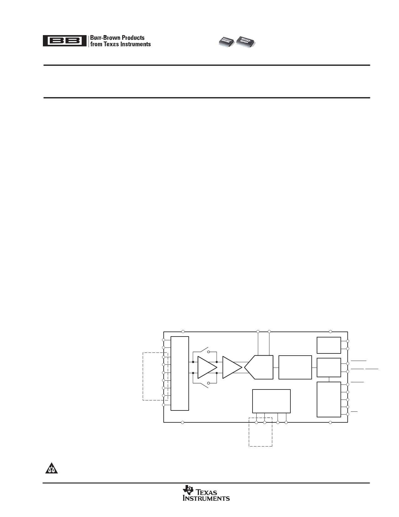
OVERVIEW
The ADS1255 and ADS1256 are very low-noise A/D
converters. The ADS1255 supports one differential or two
single-ended inputs and has two general-purpose digital
I/Os. The ADS1256 supports four differential or eight
single-ended inputs and has four general-purpose digital
I/Os. Otherwise, the two units are identical and are
referred to together in this data sheet as the ADS1255/6.
Figure 5 shows a block diagram of the ADS1256. The
input multiplexer selects which input pins are connected to
the A/D converter. Selectable current sources within the
input multiplexer can check for open- or short-circuit
conditions on the external sensor. A selectable onboard
input buffer greatly reduces the input circuitry loading by
providing up to 80MΩ of impedance. A low-noise PGA
provides a gain of 1, 2, 4, 8, 16, 32, or 64. The ADS1255/6
converter is comprised of a 4th-order, delta-sigma
modulator followed by a programmable digital filter.
ADS1255
ADS1256
SBAS288D − JUNE 2003 − REVISED AUGUST 2004
The modulator measures the amplified differential input
signal, VIN = (AINP – AINN), against the differential
reference, VREF = (VREFP − VREFN). The differential
reference is scaled internally by a factor of two so that the
full-scale input range is ±2VREF (for PGA = 1).
The digital filter receives the modulator signal and
provides a low-noise digital output. The data rate of the
filter is programmable from 2.5SPS to 30kSPS and allows
tradeoffs between resolution and speed.
Communication is done over an SPI-compatible serial
interface with a set of simple commands providing control of
the ADS1255/6. Onboard registers store the various settings
for the input multiplexer, sensor detect current sources, input
buffer enable, PGA setting, data rate, etc. Either an external
crystal or clock oscillator can be used to provide the clock
source. General-purpose digital I/Os provide static read/write
control of up to four pins. One of the pins can also be used
to supply a programmable clock output.
AIN0
AIN1
AIN2
AIN3
AIN4
AIN5
AIN6
AIN7
AINCOM
Input
Multiplexer AINP
and
Sensor
Detect
AINN
Buffer
PGA
1:64
VREFP VREFN
Σ
VREF
2
A/D
Converter
2VREF
Σ VIN • PGA 4th−Order
Modulator
Programmable
Digital Filter
Clock
Generator
Control
XTAL1/CLKIN
XTAL2
RESET
SYNC/PDWN
General
Purpose
Digital I/O
D3 D2 D1 D0/CLKOUT
ADS1256
Only
SPI
Serial
Interface
DRDY
SCLK
DIN
DOUT
CS
Figure 5. Block Diagram
11
11 Page | ||
| Páginas | Total 39 Páginas | |
| PDF Descargar | [ Datasheet ADS1255IDBR.PDF ] | |
Hoja de datos destacado
| Número de pieza | Descripción | Fabricantes |
| ADS1255IDB | Very Low Noise/ 24-Bit Analog-to-Digital Converter | Burr-Brown Corporation |
| ADS1255IDBR | Very Low Noise/ 24-Bit Analog-to-Digital Converter | Burr-Brown Corporation |
| ADS1255IDBT | Very Low Noise/ 24-Bit Analog-to-Digital Converter | Burr-Brown Corporation |
| Número de pieza | Descripción | Fabricantes |
| SLA6805M | High Voltage 3 phase Motor Driver IC. |
Sanken |
| SDC1742 | 12- and 14-Bit Hybrid Synchro / Resolver-to-Digital Converters. |
Analog Devices |
|
DataSheet.es es una pagina web que funciona como un repositorio de manuales o hoja de datos de muchos de los productos más populares, |
| DataSheet.es | 2020 | Privacy Policy | Contacto | Buscar |