|
|
|
PDF ADXL50JH Data sheet ( Hoja de datos )
| Número de pieza | ADXL50JH | |
| Descripción | Monolithic Accelerometer With Signal Conditioning | |
| Fabricantes | Analog Devices | |
| Logotipo | ||
Hay una vista previa y un enlace de descarga de ADXL50JH (archivo pdf) en la parte inferior de esta página. Total 16 Páginas | ||
|
No Preview Available !
a
Monolithic Accelerometer
With Signal Conditioning
ADXL50*
FEATURES
Complete Acceleration Measurement System
on a Single Monolithic IC
Full-Scale Measurement Range: ؎50 g
Self-Test on Digital Command
+5 V Single Supply Operation
Sensitivity Precalibrated to 19 mV/g
Internal Buffer Amplifier for User Adjustable Sensitivity
and Zero-g Level
Frequency Response: DC to 10 kHz
Post Filtering with External Passive Components
High Shock Survival: >2000 g Unpowered
Other Versions Available: ADXL05 (؎5 g)
GENERAL DESCRIPTION
The ADXL50 is a complete acceleration measurement system on
a single monolithic IC. Three external capacitors and a +5 volt
power supply are all that is required to measure accelerations up
to ± 50 g. Device sensitivity is factory trimmed to 19 mV/g,
resulting in a full-scale output swing of ± 0.95 volts for a ± 50 g
applied acceleration. Its zero g output level is +1.8 volts.
A TTL compatible self-test function can electrostatically deflect
the sensor beam at any time to verify device functionality.
For convenience, the ADXL50 has an internal buffer amplifier
with a full 0.25 V to 4.75 V output range. This may be used to
set the zero-g level and change the output sensitivity by using
external resistors. External capacitors may be added to the resis-
tor network to provide 1 or 2 poles of filtering. No external
active components are required to interface directly to most
analog-to-digital converters (ADCs) or microcontrollers.
The ADXL50 uses a capacitive measurement method. The ana-
log output voltage is directly proportional to acceleration, and is
fully scaled, referenced and temperature compensated, resulting
in high accuracy and linearity over a wide temperature range.
Internal circuitry implements a forced-balance control loop that
improves accuracy by compensating for any mechanical sensor
variations.
The ADXL50 is powered from a standard +5 V supply and is
robust for use in harsh industrial and automotive environments
and will survive shocks of more than 2000 g unpowered.
The ADXL50 is available in a hermetic 10-pin TO-100 metal
can, specified over the 0°C to +70°C commercial, and –40°C to
+85°C industrial temperature ranges. Contact factory for avail-
ability of devices specified for operation over the –40°C to
+105°C automotive temperature range.
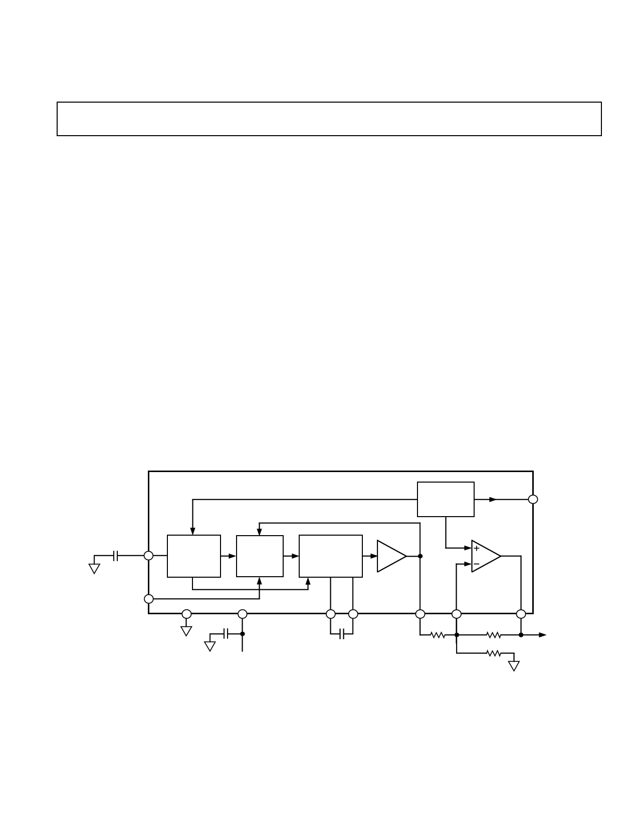
FUNCTIONAL BLOCK DIAGRAM
ADXL50
REFERENCE
+3.4V
6
VREF
OUTPUT
OSCILLATOR
DECOUPLING
CAPACITOR
4
C2
OSCILLATOR
SENSOR
SELF TEST
(ST)
7
5
COM
1
C3
+5V
+1.8V
DEMODULATOR
PREAMP
BUFFER
AMP
2
C1
3
C1
DEMODULATOR
CAPACITOR
8 10
VPR R1
VIN– R3
R2
9
VOUT
*Patents pending.
REV. B
Information furnished by Analog Devices is believed to be accurate and
reliable. However, no responsibility is assumed by Analog Devices for its
use, nor for any infringements of patents or other rights of third parties
which may result from its use. No license is granted by implication or
otherwise under any patent or patent rights of Analog Devices.
© Analog Devices, Inc., 1996
One Technology Way, P.O. Box 9106, Norwood, MA 02062-9106, U.S.A.
Tel: 617/329-4700
Fax: 617/326-8703
1 page 
ADXL50
Table I shows the percentage signals resulting from various θX
angles. Note that small errors in alignment have a negligible
effect on the output signal. A 1° error will only cause a 0.02%
error in the signal. Note, however, that a signal coming 1° off of
the transverse axis (i.e., 89° off the sensitive axis) will still con-
tribute 1.7% of its signal to the output. Thus large transverse
signals could cause output signals as large as the signals of
interest.
Table I may also be used to approximate the effect of the
ADXL50’s internal errors due to misalignment of the die to the
package. For example: a 1 degree sensor alignment error will
allow 1.7% of a transverse signal to appear at the output. In a
nonideal sensor, transverse sensitivity may also occur due to in-
herent sensor properties. That is, if the sensor physically moves
due to a force applied exactly 90° to its sensitive axis, then this
might be detected as an output signal, whereas an ideal sensor
would reject such signals. In every day use, alignment errors
may cause a small output peak with accelerations applied close
to the sensitive axis but the largest errors are normally due to
large accelerations applied close to the transverse axis.
Errors Due to Mounting Fixture Resonances
A common source of error in acceleration sensing is resonance
of the mounting fixture. For example, the circuit board that the
ADXL50 mounts to may have resonant frequencies in the same
range as the signals of interest. This could cause the signals
measured to be larger than they really are. A common solution
to this problem is to dampen these resonances by mounting the
ADXL50 near a mounting post or by adding extra screws to
hold the board more securely in place.
When testing the accelerometer in your end application, it is
recommended that you test the application at a variety of fre-
quencies in order to ensure that no major resonance problems
exist.
GLOSSARY OF TERMS
Acceleration: Change in velocity per unit time.
Acceleration Vector: Vector describing the net acceleration
acting upon the ADXL50 (AXYZ).
g: A unit of acceleration equal to the average force of gravity
occurring at the earth’s surface. A g is approximately equal to
32.17 feet/s2, or 9.807 meters/s2.
Nonlinearity: The maximum deviation of the ADXL50 output
voltage from a best fit straight line fitted to a plot of acceleration
vs. output voltage, calculated as a % of the full-scale output
voltage (@ 50 g).
Resonant Frequency: The natural frequency of vibration of
the ADXL50 sensor’s central plate (or “beam”). At its resonant
frequency of 24 kHz, the ADXL50’s moving center plate has a
peak in its frequency response with a Q of 3 or 4.
Sensitivity: The output voltage change per g unit of accelera-
tion applied, specified at the VPR pin in mV/g.
Sensitive Axis (X): The most sensitive axis of the accelerom-
eter sensor. Defined by a line drawn between the package tab
and Pin 5 in the plane of the pin circle. See Figures 2a and 2b.
Sensor Alignment Error: Misalignment between the
ADXL50’s on-chip sensor and the package axis, defined by
Pin 5 and the package tab.
Total Alignment Error: Net misalignment of the ADXL50’s
on-chip sensor and the measurement axis of the application.
This error includes errors due to sensor die alignment to the
package, and any misalignment due to installation of the sensor
package in a circuit board or module.
Transverse Acceleration: Any acceleration applied 90° to the
axis of sensitivity.
Transverse Sensitivity Error: The percent of a transverse ac-
celeration that appears at the VPR output. For example, if the
transverse sensitivity is 1%, then a +10 g transverse acceleration
will cause a 0.1 g signal to appear at VPR (1% of 10 g). Trans-
verse sensitivity can result from a sensitivity of the sensor to
transverse forces or from misalignment of the internal sensor to
its package.
Transverse Y Axis: The axis perpendicular (90°) to the pack-
age axis of sensitivity in the plane of the package pin circle. See
Figure 2.
Transverse Z Axis: The axis perpendicular (90°) to both the
package axis of sensitivity and the plane of the package pin
circle. See Figure 2.
100
90
10
0%
1V
0.5V
0.5ms
Figure 3. 500 g Shock Overload Recovery. Top Trace:
ADXL50 Output. Bottom Trace: Reference Accelerometer
Output
REV. B
–5–
5 Page 
ADXL50
As an example, if the desired span is ± 2.0 V for a = ± 50 g input,
then R3/R1 should be chosen such that
R3/R1 = VOUT Span/VPR Span = 2.00/0.95 = 2.105
(1)
where VPR span is the output from the preamplifier and VOUT
span is the buffer amplifier’s output, giving
R3 = 2.105 × R1
(2)
In noncritical applications, a resistor, R2, may simply be con-
nected between VIN– and common to provide an approximate
0 g offset level (see Figure 19). In this simplified configuration
R2 is found using:
R2 = (1.8 V × R3)/(VOUT @ 0 g – 1.8 V)
When used with a trim potentiometer, as in Figure 20, resistor
R2 sets the 0 g offset range and also sets the resolution of the
offset trim. A value of 100 kΩ is typical. Increasing R2 above
this value makes trimming the offset easier, but may not provide
enough trim range to set VOUT equal to +2.5 V for all devices.
To provide an output span of ± 2.00 V, with a 0 g output of
+2.5 V, R1 could be set to the standard value of 49.9 kΩ and
from Equation 2, R3 = 105 kΩ.
For Figure 20, the circuit transfer function is:
V OUT
=
R3
R1
(1.8
V
–
VPR
)
+
R3
R2
(1.8 V
–
VX
)
+ 1.8 V
The summing amplifier configuration allows noninteractive
trimming of offset and span. Since VPR is not always exactly
1.8 V at 0 g, it will contribute to output offset. Therefore, span
must be trimmed first, followed by 0 g offset adjustment.
LOAD DRIVE CAPABILITIES OF THE VPR AND BUFFER
OUTPUTS
The VPR and the buffer amplifier outputs are both capable of
driving a load to voltage levels approaching that of the supply
rail. However, both outputs are limited in how much current
they can supply, affecting component selection.
VPR Output
The VPR pin has the ability to source current up to 500 µA but
only has a sinking capability of 30 µA which limits its ability to
drive loads. It is recommended that the buffer amplifier be used
in most applications, to avoid loading down VPR. In standard
± 50 g applications, the resistor R1 from VPR to VIN– is recom-
mended to have a value greater than 50 kΩ to reduce loading
effects.
Capacitive loading of the VPR pin should be minimized. A load
capacitance between the VPR pin and common will introduce an
offset of approximately 1 mV for every 10 pF of load. The VPR
pin may be used to directly drive an A/D input or other source
as long as these sensitivities are taken into account. It is always
preferable to drive A/D converters or other sources using the
buffer amplifier (or an external op amp) instead of the VPR pin.
Buffer Amplifier Output
The buffer output can drive a load to within 0.25 V of either
power supply rail and is capable of driving 1000 pF capacitive
loads. Note that a capacitance connected across the buffer feed-
back resistor for low-pass filtering does not appear as a capaci-
tive load to the buffer. The buffer amplifier is limited to
sourcing or sinking a maximum of 100 µA. Component values
for the resistor network should be selected to ensure that the
buffer amplifier can drive the filter under worst case transient
conditions.
SELF-TEST FUNCTION
The digital self-test input is compatible with both CMOS and
TTL signals. A Logic “l” applied to the self-test (ST) input will
cause an electrostatic force to be applied to the sensor which
will cause it to deflect to the approximate negative full-scale out-
put of the device. Accordingly, a correctly functioning acceler-
ometer will respond by initiating an approximate –1 volt output
change at VPR. If the ADXL50 is experiencing an acceleration
when the self-test is initiated, the VPR output will equal the alge-
braic sum of the two inputs. The output will stay at the self-test
level as long as the ST input remains high and will return to the
0 g level when the ST voltage is removed.
A self-test output that varies more than ± 10% from the nominal
–1.0 V change indicates a defective beam or a circuit problem
such as an open or shorted pin or component.
Operating the ADXL50’s buffer amplifier at Gains > 2, to pro-
vide full-scale outputs of less than ± 50 g, may cause the self-test
output to overdrive the buffer into saturation. The self-test may
still be used in the case, but the change in the output must then
be monitored at the VPR pin instead of the buffer output.
Note that the value of the self-test delta is not an exact indica-
tion of the sensitivity (mV/g) of the ADXL50 and, therefore,
may not be used to calibrate the device for sensitivity error.
In critical applications, it may be desirable to monitor shifts in
the zero-g bias voltage from its initial value. A shift in the 0 g
bias level may indicate that the 0 g level has shifted which may
warrant an alarm.
POWER SUPPLY DECOUPLING
The ADXL50 power supply should be decoupled with a 0.1 µF
ceramic capacitor from +5 V pin of the ADXL50 to common
using very short component leads. For other decoupling consid-
erations, see EMI/RFI section.
OSCILLATOR DECOUPLING CAPACITOR, C2
An oscillator decoupling capacitor, C2, is used to remove
1 MHz switching transients in the sensor excitation signal, and
is required for proper operation of the ADXL50. A ceramic ca-
pacitor with a minimum value of 0.022 µF is recommended
from the oscillator decoupling capacitor pin to common. Small
amounts of capacitor leakage due to a dc resistance greater than
l MΩ will not affect operation (i.e., a high quality capacitor is
not needed here). As with the power supply bypass capacitor,
very short component leads are recommended. Although
0.022 µF is a good typical value, it may be increased for reasons
of convenience, but doing this will not improve the noise perfor-
mance of the ADXL50.
REV. B
–11–
11 Page | ||
| Páginas | Total 16 Páginas | |
| PDF Descargar | [ Datasheet ADXL50JH.PDF ] | |
Hoja de datos destacado
| Número de pieza | Descripción | Fabricantes |
| ADXL50JH | Monolithic Accelerometer With Signal Conditioning | Analog Devices |
| Número de pieza | Descripción | Fabricantes |
| SLA6805M | High Voltage 3 phase Motor Driver IC. |
Sanken |
| SDC1742 | 12- and 14-Bit Hybrid Synchro / Resolver-to-Digital Converters. |
Analog Devices |
|
DataSheet.es es una pagina web que funciona como un repositorio de manuales o hoja de datos de muchos de los productos más populares, |
| DataSheet.es | 2020 | Privacy Policy | Contacto | Buscar |