|
|
|
PDF BC847BDW1T1G Data sheet ( Hoja de datos )
| Número de pieza | BC847BDW1T1G | |
| Descripción | Dual General Purpose Transistors | |
| Fabricantes | ON Semiconductor | |
| Logotipo | ||
Hay una vista previa y un enlace de descarga de BC847BDW1T1G (archivo pdf) en la parte inferior de esta página. Total 11 Páginas | ||
|
No Preview Available !
BC846BDW1T1G,
SBC846BDW1T1G,
BC847BDW1T1G,
SBC847BDW1T1G Series,
NSVBC847BDW1T2G,
BC848CDW1T1G
Dual General Purpose
Transistors
NPN Duals
These transistors are designed for general purpose amplifier
applications. They are housed in the SOT−363/SC−88 which is
designed for low power surface mount applications.
Features
• S and NSV Prefixes for Automotive and Other Applications
Requiring Unique Site and Control Change Requirements;
AEC−Q101 Qualified and PPAP Capable
• These Devices are Pb−Free, Halogen Free/BFR Free and are RoHS
Compliant*
MAXIMUM RATINGS
Rating
Symbol BC846 BC847 BC848 Unit
Collector −Emitter Voltage
VCEO
65
45
30
V
Collector −Base Voltage
VCBO
80
50
30
V
Emitter −Base Voltage
VEBO
6.0
6.0
5.0
V
Collector Current −
Continuous
IC 100 100 100 mAdc
Stresses exceeding Maximum Ratings may damage the device. Maximum
Ratings are stress ratings only. Functional operation above the Recommended
Operating Conditions is not implied. Extended exposure to stresses above the
Recommended Operating Conditions may affect device reliability.
THERMAL CHARACTERISTICS
Characteristic
Symbol
Max
Unit
Total Device Dissipation Per Device
FR−5 Board (Note 1)
TA = 25°C
Derate Above 25°C
PD
380 mW
250 mW/°C
3.0 mW/°C
Thermal Resistance,
Junction to Ambient
RqJA
°C/W
328
Junction and Storage Temperature
Range
TJ, Tstg − 55 to +150
°C
1. FR−5 = 1.0 x 0.75 x 0.062 in
*For additional information on our Pb−Free strategy and soldering details, please
download the ON Semiconductor Soldering and Mounting Techniques
Reference Manual, SOLDERRM/D.
http://onsemi.com
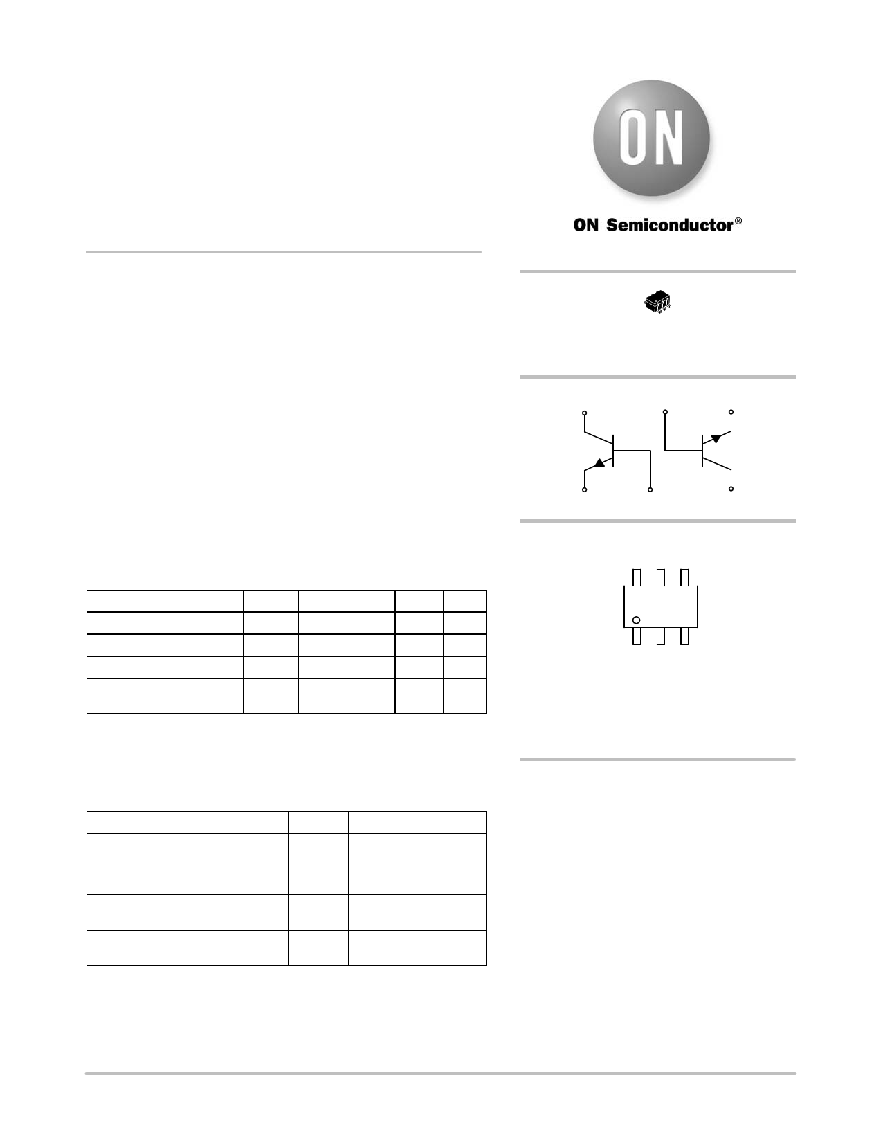
SOT−363
CASE 419B
STYLE 1
(3) (2) (1)
Q1 Q2
(4) (5)
(6)
MARKING DIAGRAM
6
1x MG
G
1
1x = Specific Device Code
x = B, F, G, L
M = Date Code
G = Pb−Free Package
(Note: Microdot may be in either location)
ORDERING INFORMATION
See detailed ordering and shipping information in the package
dimensions section on page 6 of this data sheet.
© Semiconductor Components Industries, LLC, 2012
September, 2012 − Rev. 9
1
Publication Order Number:
BC846BDW1T1/D
1 page 
BC846BDW1T1G, SBC846BDW1T1G, BC847BDW1T1G, SBC847BDW1T1G Series,
NSVBC847BDW1T2G, BC848CDW1T1G
TYPICAL CHARACTERISTICS − BC847BDW1T1G, SBC847BDW1T1G, NSVBC847BDW1T2G
600
500 150°C
VCE = 5 V
400
300 25°C
200 −55°C
100
0
0.0001
0.001
0.01
0.1
IC, COLLECTOR CURRENT (A)
Figure 12. DC Current Gain at VCE = 5 V
1
600
500 150°C
VCE = 10 V
400
25°C
300
200 −55°C
100
0
0.0001
0.001
0.01
0.1
IC, COLLECTOR CURRENT (A)
Figure 13. DC Current Gain at VCE = 10 V
1
0.25
IC/IB = 10
0.20
0.15
0.10
0.05
0.000.0001
25°C
150°C
−55°C
0.001
0.01
IC, COLLECTOR CURRENT (A)
Figure 14. VCE at IC/IB = 10
0.30
0.25
IC/IB = 20
0.20
0.15
0.10
25°C
150°C
0.05
0.1 0.000.0001
−55°C
0.001
0.01
IC, COLLECTOR CURRENT (A)
Figure 15. VCE at IC/IB = 20
0.1
1.20
1.00
IC/IB = 10
0.80
0.60
0.40
−55°C
25°C
150°C
0.20
0.00
0.0001
0.001
0.01
IC, COLLECTOR CURRENT (A)
Figure 16. VBE(sat) at IC/IB = 10
1.20
1.00
IC/IB = 20
0.80 −55°C
25°C
0.60
0.40 150°C
0.20
0.00
0.1 0.0001
0.001
0.01
IC, COLLECTOR CURRENT (A)
Figure 17. VBE(sat) at IC/IB = 20
0.1
http://onsemi.com
5
5 Page 
BC846BDW1T1G, SBC846BDW1T1G, BC847BDW1T1G, SBC847BDW1T1G Series,
NSVBC847BDW1T2G, BC848CDW1T1G
PACKAGE DIMENSIONS
SC−88 (SC70−6/SOT−363)
CASE 419B−02
D ISSUE W
e
654
NOTES:
1. DIMENSIONING AND TOLERANCING PER ANSI
Y14.5M, 1982.
2. CONTROLLING DIMENSION: INCH.
3. 419B−01 OBSOLETE, NEW STANDARD 419B−02.
HE −E−
123
b 6 PL
0.2 (0.008) M E M
A3
A
A1 L
C
MILLIMETERS
INCHES
DIM MIN NOM MAX MIN NOM MAX
A 0.80 0.95 1.10 0.031 0.037 0.043
A1 0.00 0.05 0.10 0.000 0.002 0.004
A3 0.20 REF
0.008 REF
b 0.10 0.21 0.30 0.004 0.008 0.012
C 0.10 0.14 0.25 0.004 0.005 0.010
D 1.80 2.00 2.20 0.070 0.078 0.086
E 1.15 1.25 1.35 0.045 0.049 0.053
e 0.65 BSC
0.026 BSC
L 0.10 0.20 0.30 0.004 0.008 0.012
HE 2.00 2.10 2.20 0.078 0.082 0.086
STYLE 1:
PIN 1. EMITTER 2
2. BASE 2
3. COLLECTOR 1
4. EMITTER 1
5. BASE 1
6. COLLECTOR 2
SOLDERING FOOTPRINT*
0.50
0.0197
0.40
0.0157
0.65
0.025
0.65
0.025
1.9
0.0748
ǒ ǓSCALE 20:1
mm
inches
*For additional information on our Pb−Free strategy and soldering
details, please download the ON Semiconductor Soldering and
Mounting Techniques Reference Manual, SOLDERRM/D.
ON Semiconductor and
are registered trademarks of Semiconductor Components Industries, LLC (SCILLC). SCILLC reserves the right to make changes without further notice
to any products herein. SCILLC makes no warranty, representation or guarantee regarding the suitability of its products for any particular purpose, nor does SCILLC assume any liability
arising out of the application or use of any product or circuit, and specifically disclaims any and all liability, including without limitation special, consequential or incidental damages.
“Typical” parameters which may be provided in SCILLC data sheets and/or specifications can and do vary in different applications and actual performance may vary over time. All
operating parameters, including “Typicals” must be validated for each customer application by customer’s technical experts. SCILLC does not convey any license under its patent rights
nor the rights of others. SCILLC products are not designed, intended, or authorized for use as components in systems intended for surgical implant into the body, or other applications
intended to support or sustain life, or for any other application in which the failure of the SCILLC product could create a situation where personal injury or death may occur. Should
Buyer purchase or use SCILLC products for any such unintended or unauthorized application, Buyer shall indemnify and hold SCILLC and its officers, employees, subsidiaries, affiliates,
and distributors harmless against all claims, costs, damages, and expenses, and reasonable attorney fees arising out of, directly or indirectly, any claim of personal injury or death
associated with such unintended or unauthorized use, even if such claim alleges that SCILLC was negligent regarding the design or manufacture of the part. SCILLC is an Equal
Opportunity/Affirmative Action Employer. This literature is subject to all applicable copyright laws and is not for resale in any manner.
PUBLICATION ORDERING INFORMATION
LITERATURE FULFILLMENT:
Literature Distribution Center for ON Semiconductor
P.O. Box 5163, Denver, Colorado 80217 USA
Phone: 303−675−2175 or 800−344−3860 Toll Free USA/Canada
Fax: 303−675−2176 or 800−344−3867 Toll Free USA/Canada
Email: [email protected]
N. American Technical Support: 800−282−9855 Toll Free
USA/Canada
Europe, Middle East and Africa Technical Support:
Phone: 421 33 790 2910
Japan Customer Focus Center
Phone: 81−3−5817−1050
http://onsemi.com
11
ON Semiconductor Website: www.onsemi.com
Order Literature: http://www.onsemi.com/orderlit
For additional information, please contact your local
Sales Representative
BC846BDW1T1/D
11 Page | ||
| Páginas | Total 11 Páginas | |
| PDF Descargar | [ Datasheet BC847BDW1T1G.PDF ] | |
Hoja de datos destacado
| Número de pieza | Descripción | Fabricantes |
| BC847BDW1T1 | Dual General Purpose Transistors | ON Semiconductor |
| BC847BDW1T1G | Dual General Purpose Transistors | ON Semiconductor |
| Número de pieza | Descripción | Fabricantes |
| SLA6805M | High Voltage 3 phase Motor Driver IC. |
Sanken |
| SDC1742 | 12- and 14-Bit Hybrid Synchro / Resolver-to-Digital Converters. |
Analog Devices |
|
DataSheet.es es una pagina web que funciona como un repositorio de manuales o hoja de datos de muchos de los productos más populares, |
| DataSheet.es | 2020 | Privacy Policy | Contacto | Buscar |