|
|
PDF DS1302 Data sheet ( Hoja de datos )
| Número de pieza | DS1302 | |
| Descripción | Trickle-Charge Timekeeping Chip | |
| Fabricantes | Maxim Integrated | |
| Logotipo |  |
|
Hay una vista previa y un enlace de descarga de DS1302 (archivo pdf) en la parte inferior de esta página. Total 13 Páginas | ||
|
No Preview Available !
DS1302
Trickle-Charge Timekeeping Chip
BENEFITS AND FEATURES
Completely Manages All Timekeeping Functions
o Real-Time Clock Counts Seconds,
Minutes, Hours, Date of the Month, Month,
Day of the Week, and Year with Leap-Year
Compensation Valid Up to 2100
o 31 x 8 Battery-Backed General-Purpose
RAM
Simple Serial Port Interfaces to Most
Microcontrollers
o Simple 3-Wire Interface
o TTL-Compatible (VCC = 5V)
o Single-Byte or Multiple-Byte (Burst Mode)
Data Transfer for Read or Write of Clock or
RAM Data
Low Power Operation Extends Battery Backup
Run Time
o 2.0V to 5.5V Full Operation
o Uses Less Than 300nA at 2.0V
8-Pin DIP and 8-Pin SO Minimizes Required
Space
Optional Industrial Temperature Range: -40°C
to +85°C Supports Operation in a Wide Range
of Applications
Underwriters Laboratories® (UL) Recognized
PIN CONFIGURATIONS
TOP VIEW
VCC2
X1
X2
GND
1
2
3
4
8 VCC1
7 SCLK
6 I/O
5 CE
DIP (300mils)
VCC2
X1
X2
GND
1
2
3
4
8 VCC1
7 SCLK
6 I/O
5 CE
SO (208 mils/150 mils)
ORDERING INFORMATION
PART
TEMP RANGE
DS1302+
0°C to +70°C
DS1302N+
-40°C to +85°C
DS1302S+
0°C to +70°C
DS1302SN+
-40°C to +85°C
DS1302Z+
0°C to +70°C
DS1302ZN+
-40°C to +85°C
PIN-PACKAGE
8 PDIP (300 mils)
8 PDIP (300 mils)
8 SO (208 mils)
8 SO (208 mils)
8 SO (150 mils)
8 SO (150 mils)
TOP MARK*
DS1302
DS1302
DS1302S
DS1302S
DS1302Z
DS1302ZN
+Denotes a lead-free/RoHS-compliant package.
*An N anywhere on the top mark indicates an industrial temperature grade device. A + anywhere on the top mark indicates a lead-free device.
UL is a registered trademark of Underwriters Laboratories, Inc.
1 of 13
REV: 3/15
1 page 
DS1302 Trickle-Charge Timekeeping Chip
OSCILLATOR CIRCUIT
The DS1302 uses an external 32.768kHz crystal. The oscillator circuit does not require any external resistors or
capacitors to operate. Table 1 specifies several crystal parameters for the external crystal. Figure 1 shows a
functional schematic of the oscillator circuit. If using a crystal with the specified characteristics, the startup time is
usually less than one second.
CLOCK ACCURACY
The accuracy of the clock is dependent upon the accuracy of the crystal and the accuracy of the match between
the capacitive load of the oscillator circuit and the capacitive load for which the crystal was trimmed. Additional
error will be added by crystal frequency drift caused by temperature shifts. External circuit noise coupled into the
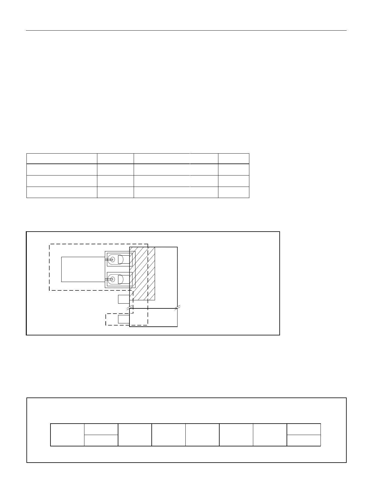
oscillator circuit may result in the clock running fast. Figure 2 shows a typical PC board layout for isolating the
crystal and oscillator from noise. Refer to Application Note 58: Crystal Considerations for Dallas Real-Time Clocks
for detailed information.
Table 1. Crystal Specifications*
PARAMETER
SYMBOL MIN
Nominal Frequency
fO
Series Resistance
ESR
Load Capacitance
CL
TYP
32.768
6
MAX
45
UNITS
kHz
kΩ
pF
*The crystal, traces, and crystal input pins should be isolated from RF generating signals. Refer to
Application Note 58: Crystal Considerations for Dallas Real-Time Clocks for additional specifications.
Figure 2. Typical PC Board Layout for Crystal
LOCAL GROUND PLANE (LAYER 2)
CRYSTAL
X1
X2
NOTE: AVOID ROUTING SIGNALS IN THE
CROSSHATCHED AREA (UPPER LEFT-
HAND QUADRANT) OF THE PACKAGE
UNLESS THERE IS A GROUND PLANE
BETWEEN THE SIGNAL LINE AND THE
PACKAGE.
GND
COMMAND BYTE
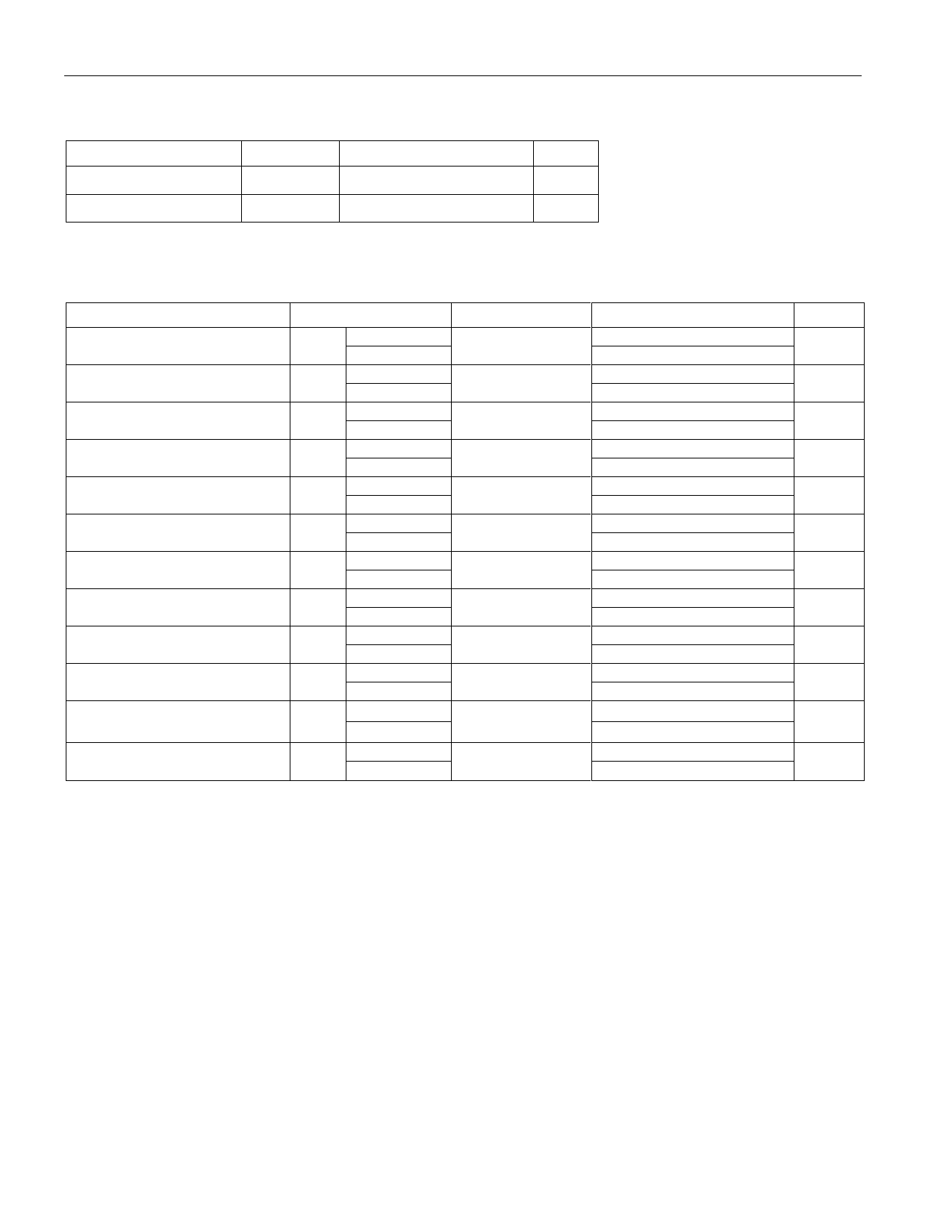
Figure 3 shows the command byte. A command byte initiates each data transfer. The MSB (bit 7) must be a logic
1. If it is 0, writes to the DS1302 will be disabled. Bit 6 specifies clock/calendar data if logic 0 or RAM data if logic 1.
Bits 1 to 5 specify the designated registers to be input or output, and the LSB (bit 0) specifies a write operation
(input) if logic 0 or read operation (output) if logic 1. The command byte is always input starting with the LSB (bit 0).
Figure 3. Address/Command Byte
76543210
RAM
RD
1 CK A4 A3 A2 A1 A0 WR
5 of 13
5 Page 
CAPACITANCE
(TA = +25°C)
PARAMETER
Input Capacitance
I/O Capacitance
DS1302 Trickle-Charge Timekeeping Chip
SYMBOL MIN TYP MAX UNITS
CI 10 pF
CI/O 15 pF
AC ELECTRICAL CHARACTERISTICS
(TA = 0°C to +70°C or TA = -40°C to +85°C.) (Note 1)
PARAMETER
SYMBOL
Data to CLK Setup
CLK to Data Hold
CLK to Data Delay
CLK Low Time
CLK High Time
CLK Frequency
CLK Rise and Fall
CE to CLK Setup
CLK to CE Hold
CE Inactive Time
CE to I/O High Impedance
SCLK to I/O High Impedance
tDC
tCDH
tCDD
tCL
tCH
tCLK
tR, tF
tCC
tCCH
tCWH
tCDZ
tCCZ
VCC = 2.0V
VCC = 5V
VCC = 2.0V
VCC = 5V
VCC = 2.0V
VCC = 5V
VCC = 2.0V
VCC = 5V
VCC = 2.0V
VCC = 5V
VCC = 2.0V
VCC = 5V
VCC = 2.0V
VCC = 5V
VCC = 2.0V
VCC = 5V
VCC = 2.0V
VCC = 5V
VCC = 2.0V
VCC = 5V
VCC = 2.0V
VCC = 5V
VCC = 2.0V
VCC = 5V
CONDITIONS
(Note 6)
(Note 6)
(Notes 6, 7, 8)
(Note 6)
(Note 6)
(Note 6)
(Note 6)
(Note 6)
(Note 6)
(Note 6)
(Note 6)
MIN TYP MAX UNITS
200
50
ns
280
70
ns
800
200
ns
1000
250
ns
1000
250
ns
DC
0.5
2.0
MHz
2000
500
ns
4
1
µs
240
60
ns
4
1
µs
280
70 ns
280
70
ns
Note 1:
Note 2:
Note 3:
Note 4:
Note 5:
Note 6:
Note 7:
Note 8:
Note 9:
Note 10:
Note 11:
Note 12:
Note 13:
Limits at -40°C are guaranteed by design and are not production tested.
All voltages are referenced to ground.
ICC1T and ICC2T are specified with I/O open, CE and SCLK set to a logic 0.
ICC1A and ICC2A are specified with the I/O pin open, CE high, SCLK = 2MHz at VCC = 5V; SCLK = 500kHz, VCC = 2.0V.
CE, SCLK, and I/O all have 40kΩ pulldown resistors to ground.
Measured at VIH = 2.0V or VIL = 0.8V and 10ns maximum rise and fall time.
Measured at VOH = 2.4V or VOL = 0.4V.
Load capacitance = 50pF.
ICC1S and ICC2S are specified with CE, I/O, and SCLK open.
VCC = VCC2, when VCC2 > VCC1 + 0.2V; VCC = VCC1, when VCC1 > VCC2.
VCC2 = 0V.
VCC1 = 0V.
Typical values are at +25°C.
11 of 13
11 Page | ||
| Páginas | Total 13 Páginas | |
| PDF Descargar | [ Datasheet DS1302.PDF ] | |
Hoja de datos destacado
| Número de pieza | Descripción | Fabricantes |
| DS1300-3 | AC-DC / Distributed Power Front-End 2U | Emerson |
| DS1302 | Trickle-Charge Timekeeping Chip | Maxim Integrated |
| DS1302 | Trickle Charge Timekeeping Chip | Dallas |
| DS1302 | Trickle Charge Timekeeping Chip | TGS |
| Número de pieza | Descripción | Fabricantes |
| SLA6805M | High Voltage 3 phase Motor Driver IC. |
Sanken |
| SDC1742 | 12- and 14-Bit Hybrid Synchro / Resolver-to-Digital Converters. |
Analog Devices |
|
DataSheet.es es una pagina web que funciona como un repositorio de manuales o hoja de datos de muchos de los productos más populares, |
| DataSheet.es | 2020 | Privacy Policy | Contacto | Buscar |
