|
|
|
PDF ADuC832 Data sheet ( Hoja de datos )
| Número de pieza | ADuC832 | |
| Descripción | MicroConverter 12-Bit ADCs and DACs | |
| Fabricantes | Analog Devices | |
| Logotipo | ||
Hay una vista previa y un enlace de descarga de ADuC832 (archivo pdf) en la parte inferior de esta página. Total 30 Páginas | ||
|
No Preview Available !
Data Sheet
MicroConverter, 12-Bit ADCs and DACs
with Embedded 62 kB Flash MCU
ADuC832
FEATURES
ANALOG I/O
8-channel, 247 kSPS, 12-Bit ADC
DC performance: ±1 LSB INL
AC performance: 71 dB SNR
DMA controller for high speed ADC-to-RAM capture
2 12-bit (monotonic) voltage output DACs
Dual output PWM/Σ-Δ DACs
On-chip temperature sensor function: ±3°C
On-chip voltage reference
Memory
62 kB on-chip Flash/EE program memory
4 kB on-chip Flash/EE data memory
Flash/EE, 100 Yr retention, 100,000 cycles of endurance
2304 bytes on-chip data RAM
8051-based core
8051-compatible instruction set (16 MHz maximum)
32 kHz external crystal, on-chip programmable PLL
12 interrupt sources, 2 priority levels
Dual data pointer
Extended 11-bit stack pointer
On-chip peripherals
Time interval counter (TIC)
UART, I2C, and SPI Serial I/O
Watchdog timer (WDT), power supply monitor (PSM)
Power
Specified for 3 V and 5 V operation
Normal, idle, and power-down modes
Power-down: 25 μA @ 3 V with wake-up timer running
APPLICATIONS
Optical networking—laser power control
Base station systems
Precision instrumentation, smart sensors
Transient capture systems
DAS and communications systems
Upgrade to ADuC812 systems; runs from 32 kHz
External crystal with on-chip PLL.
Also available: ADuC831 pin-compatible upgrade to
existing ADuC812 systems that require additional
code or data memory; runs from 1 MHz to 16 MHz
External crystal
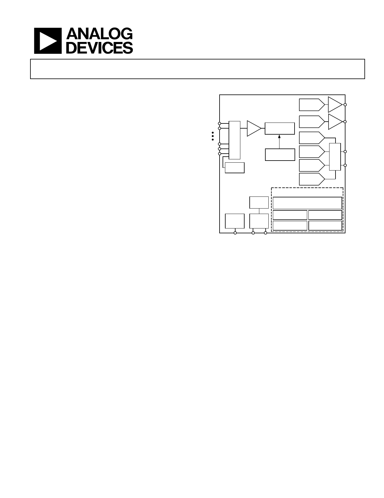
FUNCTIONAL BLOCK DIAGRAM
ADuC832
12-BIT
DAC
BUF
DAC0
ADC0
ADC1
ADC5
ADC6
ADC7
MUX
T/H
TEMP
SENSOR
12-BIT ADC
HARDWARE
CALIBRATON
12-BIT
DAC
16-BIT
Σ-∆ DAC
16-BIT
Σ-∆ DAC
16-BIT
PWM
16-BIT
PWM
BUF
DAC1
MUX
PWM0
PWM1
INTERNAL
BAND GAP
VREF
PLL
OSC
8051-BASED MCU WITH ADDITIONAL
PERIPHERALS
62 kB FLASH/EE PROGRAM MEMORY
4 kB FLASH/EE DATA MEMORY
2304 BYTES USER RAM
3 × 16-BIT TIMERS POWER SUPPLY MON
1 × REAL-TIME CLOCK WATCHDOG TIMER
4 × PARALLEL
PORTS
UART, I2C, AND SPI
SERIAL I/O
VREF
XTAL1 XTAL2
Figure 1.
GENERAL DESCRIPTION
The ADuC832 is a complete, smart transducer front end,
integrating a high performance self-calibrating multichannel
12-bit ADC, dual 12-bit DACs, and programmable 8-bit MCU
on a single chip.
The device operates from a 32 kHz crystal with an on-chip PLL,
generating a high frequency clock of 16.78 MHz. This clock is,
in turn, routed through a programmable clock divider from
which the MCU core clock operating frequency is generated.
The microcontroller core is an 8052 and is therefore 8051
instruction set compatible with 12 core clock periods per
machine cycle. 62 kB of nonvolatile Flash/EE program memory are
provided on chip. There are also 4 kB of nonvolatile Flash/EE data
memory, 256 bytes of RAM, and 2 kB of extended RAM integrated
on chip.
The ADuC832 also incorporates additional analog functionality
with two 12-bit DACs, a power supply monitor, and a band gap
reference. On-chip digital peripherals include two 16-bit Σ-Δ
DACs, a dual-output 16-bit PWM, a watchdog timer, time
interval counter, three timers/counters, Timer 3 for baud rate
generation, and serial I/O ports (SPI, I2C®, and UART).
Rev. C
Document Feedback
Information furnished by Analog Devices is believed to be accurate and reliable. However, no
responsibility is assumed by Analog Devices for its use, nor for any infringements of patents or other
rights of third parties that may result from its use. Specifications subject to change without notice. No
license is granted by implication or otherwise under any patent or patent rights of Analog Devices.
Trademarksandregisteredtrademarksarethepropertyoftheirrespectiveowners.
One Technology Way, P.O. Box 9106, Norwood, MA 02062-9106, U.S.A.
Tel: 781.329.4700 ©2002–2016 Analog Devices, Inc. All rights reserved.
Technical Support
www.analog.com
1 page 
ADuC832
REVISION HISTORY
5/2016—Rev. B to Rev. C
Changes to EPAD, Description Column, Table 13..................... 21
Updated Outline Dimensions ....................................................... 89
Changes to Ordering Guide .......................................................... 89
4/2013—Rev. A to Rev. B
Updated Outline Dimensions ....................................................... 89
Changes to Ordering Guide .......................................................... 89
9/2009—Rev. 0 to Rev. A
Changes to Figure 1.......................................................................... 1
Changed 16.77 MHz to 16.78 MHz Throughout ......................... 1
Changes to Reference Input/Output, Output Voltage Parameter,
Endnote 19, and Endnote 20, Table 1 ............................................ 9
Moved Timing Specifications Section ......................................... 10
Changes to Figure 3........................................................................ 10
Changes to Table 3.......................................................................... 11
Changes to Table 4.......................................................................... 12
Changes to Table 5.......................................................................... 13
Changes to Table 11........................................................................ 19
Changes to Figure 15 and Table 13............................................... 21
Changes to Figure 16, Figure 17, Figure 20, and Figure 21....... 26
Added Explanation of Typical Performance Plots Section ....... 30
Changes to Flash/EE Program Memory, Flash/EE Data
Memory, and General-Purpose RAM Sections.......................... 31
Changes to Figure 36...................................................................... 34
Changes to Figure 39 and Figure 40............................................. 39
Changes to Table 20........................................................................ 40
Data Sheet
Changes to A Typical DMA Mode Configuration Example
Section.............................................................................................. 41
Changed 16.777216 MHz to 16.78 MHz Throughout .............. 41
Changes to Table 21 ....................................................................... 48
Changes to Using the DAC Section and Figure 52 .................... 52
Changes to Figure 54 Caption ...................................................... 53
Changes to Figure 56...................................................................... 55
Changed 16.77 MHz to 16.78 MHz ............................................. 56
Changes to Figure 60...................................................................... 57
Changes to Table 31 ....................................................................... 63
Deleted Figure 65 and Figure 66; Renumbered Sequentially ... 66
Deleted ASPIRE—IDE Section..................................................... 66
Deleted Figure 67............................................................................ 67
Changes to Table 34 ....................................................................... 67
Changes to Figure 68, Figure 69, Figure 70, and Table 35 ........ 68
Changes to Figure 84...................................................................... 78
Changes to External Memory Interface Section ........................ 82
Changes to Power Supplies Section ............................................. 83
Changes to Table 50 ....................................................................... 84
Changes to Figure 94...................................................................... 86
Changes to Single-Pin Emulation Mode Section ....................... 87
Changes to QuickStart Development System Section and
QuickStart Plus Development System Section ........................... 88
Updated Outline Dimensions....................................................... 89
Changes to Ordering Guide .......................................................... 89
11/2002—Revision 0: Initial Version
Rev. C | Page 4 of 92
5 Page 
ADuC832
Data Sheet
TIMING SPECIFICATIONS
AVDD = 2.7 V to 3.6 V or 4.75 V to 5.25 V, DVDD = 2.7 V to 3.6 V or 4.75 V to 5.25 V; all specifications TMIN to TMAX, unless otherwise noted.
Table 2. Clock Input (External Clock Applied on XTAL1)
Parameter1, 2, 3
tCK
tCKL
tCKH
tCKR
tCKF
1/tCORE
tCORE
tCYC
Description
XTAL1 period (see Figure 3)
XTAL1 width low (see Figure 3)
XTAL1 width high (see Figure 3)
XTAL1 rise time (see Figure 3)
XTAL1 fall time (see Figure 3)
ADuC832 core clock frequency4
ADuC832 core clock period5
ADuC832 machine cycle time6
Min
0.131
0.72
32.768 kHz External Crystal
Typ Max
30.52
15.16
15.16
20
20
16.78
0.476
5.7 91.55
Unit
μs
μs
μs
ns
ns
MHz
μs
μs
1 AC inputs during testing are driven at DVDD − 0.5 V for a Logic 1 and 0.45 V for a Logic 0. Timing measurements are made at VIH minimum for a Logic 1 and VIL maximum for
a Logic 0, as shown in Figure 4.
2 For timing purposes, a port pin is no longer floating when a 100 mV change from load voltage occurs. A port pin begins to float when a 100 mV change from the
loaded VOH/VOL level occurs, as shown in Figure 4.
3 CLOAD for all outputs = 80 pF, unless otherwise noted.
4 The ADuC832 internal PLL locks onto a multiple (512 times) the external crystal frequency of 32.768 kHz to provide a stable 16.78 MHz internal clock for the system.
The core can operate at this frequency or at a binary submultiple called Core_CLK, selected via the PLLCON SFR.
5 This number is measured at the default Core_CLK operating frequency of 2.09 MHz.
6 ADuC832 machine cycle time is nominally defined as 12/Core_CLK.
tCKH
tCKR
DVDD –0.5V
0.45V
tCKL
tCK
Figure 3. XTAL1 Input
tCKF
0.2DVDD + 0.9V
TEST POINTS
0.2DVDD – 0.1V
VLOAD – 0.1V
VLOAD
VLOAD + 0.1V
TIMING
REFERENCE
POINTS
Figure 4. Timing Waveform Characteristics
VLOAD – 0.1V
VLOAD
VLOAD + 0.1V
Rev. C | Page 10 of 92
11 Page | ||
| Páginas | Total 30 Páginas | |
| PDF Descargar | [ Datasheet ADuC832.PDF ] | |
Hoja de datos destacado
| Número de pieza | Descripción | Fabricantes |
| ADUC831 | MicroConverter/ 12-Bit ADCs and DACs with Embedded 62 kBytes Flash MCU | Analog Devices |
| ADUC831BCP | MicroConverter/ 12-Bit ADCs and DACs with Embedded 62 kBytes Flash MCU | Analog Devices |
| ADUC831BS | MicroConverter/ 12-Bit ADCs and DACs with Embedded 62 kBytes Flash MCU | Analog Devices |
| ADuC832 | MicroConverter 12-Bit ADCs and DACs | Analog Devices |
| Número de pieza | Descripción | Fabricantes |
| SLA6805M | High Voltage 3 phase Motor Driver IC. |
Sanken |
| SDC1742 | 12- and 14-Bit Hybrid Synchro / Resolver-to-Digital Converters. |
Analog Devices |
|
DataSheet.es es una pagina web que funciona como un repositorio de manuales o hoja de datos de muchos de los productos más populares, |
| DataSheet.es | 2020 | Privacy Policy | Contacto | Buscar |