|
|
|
PDF DMG4932LSD Data sheet ( Hoja de datos )
| Número de pieza | DMG4932LSD | |
| Descripción | ASYMETRICAL DUAL N-CHANNEL ENHANCEMENT MODE MOSFET | |
| Fabricantes | Diodes | |
| Logotipo | ||
Hay una vista previa y un enlace de descarga de DMG4932LSD (archivo pdf) en la parte inferior de esta página. Total 9 Páginas | ||
|
No Preview Available !
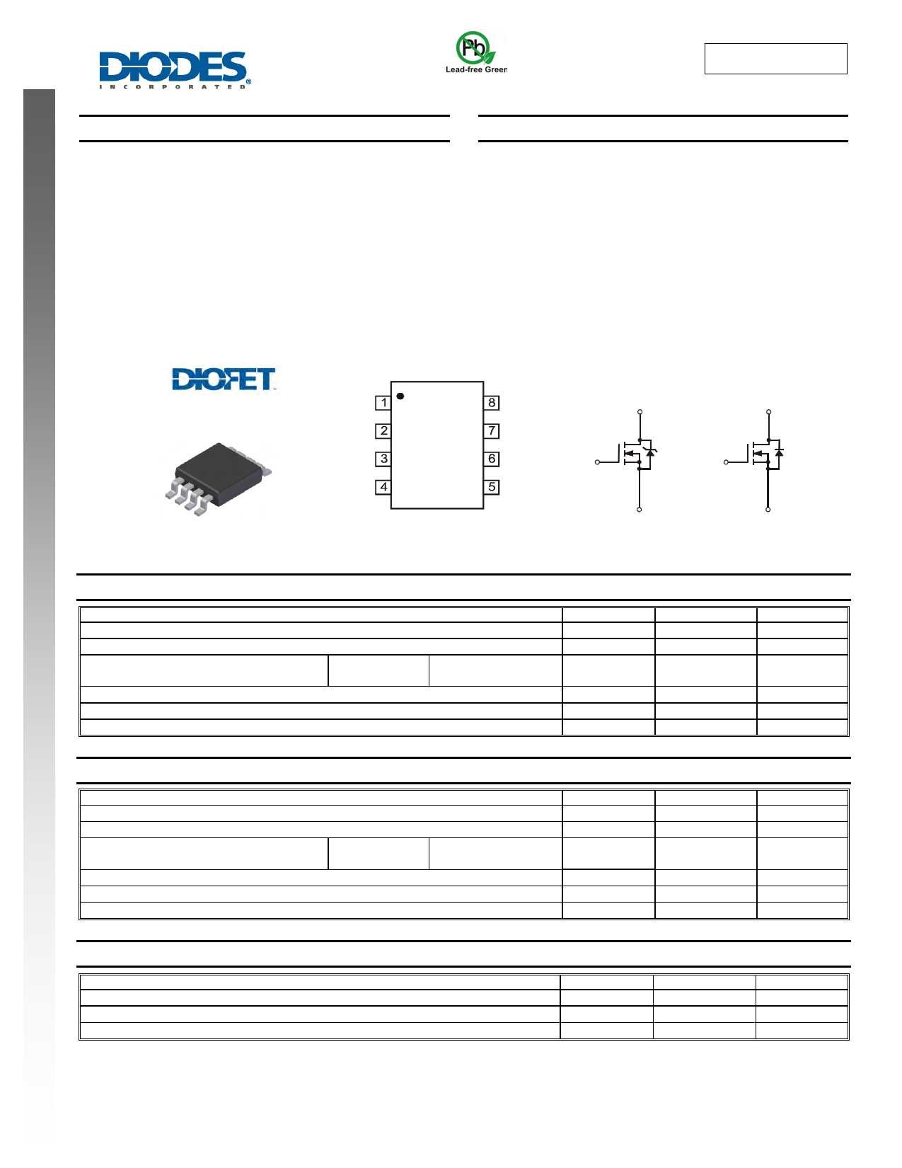
DMG4932LSD
ASYMETRICAL DUAL N-CHANNEL ENHANCEMENT MODE MOSFET
Features
• High Density UMOS with Schottky Barrier Diode
• Low Leakage Current at High Temp.
• High Conversion Efficiency
• Low On-Resistance
• Low Input Capacitance
• Fast Switching Speed
• Utilizes Diodes’ Monolithic DIOFET Technology to Increase
Conversion Efficiency
• 100% UIS and Rg Tested
• Lead Free By Design/RoHS Compliant (Note 1)
• "Green" Device (Note 2)
• Qualified to AEC-Q101 Standards for High Reliability
Mechanical Data
• Case: SO-8
• Case Material: Molded Plastic, “Green” Molding Compound.
UL Flammability Classification Rating 94V-0
• Moisture Sensitivity: Level 1 per J-STD-020
• Terminal Connections: See Diagram Below
• Marking Information: See Page 8
• Ordering Information: See Page 8
• Weight: 0.072 grams (approximate)
Diodes Schottky Integrated MOSFET
D2
D2
G1
S1
G2
S2/D1
S2/D1
S2/D1
Top View
Top View
Internal Schematic
Q1
D1
Q2
D2
G1 G2
S1
N-Channel MOSFET
S2
N-Channel MOSFET
Maximum Ratings – Q1 @TA = 25°C unless otherwise specified
Characteristic
Drain-Source Voltage
Gate-Source Voltage
Continuous Drain Current (Note 3)
Steady
State
Pulsed Drain Current (Note 4)
Avalanche Current (Notes 4 & 5)
Repetitive Avalanche Energy (Notes 4 & 5) L = 0.3mH
TA = 25°C
TA = 85°C
Symbol
VDSS
VGSS
ID
IDM
IAR
EAR
Value
30
±12
9.5
7.2
40
13
25.4
Unit
V
V
A
A
A
mJ
Maximum Ratings – Q2 @TA = 25°C unless otherwise specified
Characteristic
Drain-Source Voltage
Gate-Source Voltage
Continuous Drain Current (Note 3)
Steady
State
Pulsed Drain Current (Note 4)
Avalanche Current (Notes 4 & 5)
Repetitive Avalanche Energy (Notes 4 & 5) L = 0.3mH
TA = 25°C
TA = 85°C
Symbol
VDSS
VGSS
ID
IDM
IAR
EAR
Value
30
±25
9.5
7.5
40
13
25.4
Unit
V
V
A
A
A
mJ
Thermal Characteristics
Characteristic
Power Dissipation (Note 3)
Thermal Resistance, Junction to Ambient @TA = 25°C (Note 3)
Operating and Storage Temperature Range
Symbol
PD
RθJA
TJ, TSTG
Value
1.19
107
-55 to +150
Unit
W
°C/W
°C
Notes:
1. No purposefully added lead.
2. Diodes Inc.'s "Green" policy can be found on our website at http://www.diodes.com/products/lead_free/index.php.
3. Device mounted on FR-4 PCB with minimum recommended pad layout. The value in any given application depends on the user’s specific board design.
4. Repetitive rating, pulse width limited by junction temperature.
5. IAR and EAR rating are based on low frequency and duty cycles to keep TJ = 25°C
DMG4932LSD
Document number: DS32119 Rev. 4 - 2
1 of 9
www.diodes.com
August 2010
© Diodes Incorporated
1 page 
DMG4932LSD
Electrical Characteristics – Q2 @TA = 25°C unless otherwise specified
Characteristic
OFF CHARACTERISTICS (Note 6)
Drain-Source Breakdown Voltage
Zero Gate Voltage Drain Current
Gate-Source Leakage
ON CHARACTERISTICS (Note 6)
Gate Threshold Voltage
Static Drain-Source On-Resistance
Symbol
BVDSS
IDSS
IGSS
VGS(th)
RDS (ON)
Min
30
-
-
-
1.0
-
Typ
-
-
-
-
-
12
16
Forward Transfer Admittance
Diode Forward Voltage
DYNAMIC CHARACTERISTICS (Note 7)
Input Capacitance
Output Capacitance
Reverse Transfer Capacitance
Gate Resistance
Total Gate Charge (4.5V)
Total Gate Charge (10V)
Gate-Source Charge
Gate-Drain Charge
Turn-On Delay Time
Turn-On Rise Time
Turn-Off Delay Time
Turn-Off Fall Time
|Yfs|
VSD
Ciss
Coss
Crss
Rg
Qg
Qg
Qgs
Qgd
tD(on)
tr
tD(off)
tf
-8
- 0.65
- 675
- 98
- 90
- 1.6
- 7.8
- 16.0
- 1.9
- 2.6
- 5.05
- 9.21
- 20.76
- 4.94
Notes:
6. Short duration pulse test used to minimize self-heating effect.
7. Guaranteed by design. Not subject to production testing.
Max
-
1
+100
-800
2.3
15.8
23
-
1.0
-
-
-
-
-
-
-
-
-
-
-
-
Unit Test Condition
V VGS = 0V, ID = 250μA
μA VDS = 30V, VGS = 0V
nA VGS = +25V, VDS = 0V
VGS = -25V, VDS = 0V
V VDS = VGS, ID = 250μA
mΩ VGS = 10V, ID = 9A
VGS = 4.5V, ID = 7A
S VDS = 10V, ID = 9A
V VGS = 0V, IS = 1A
pF
pF
VDS = 15V, VGS = 0V,
f = 1.0MHz
pF
Ω VDS = 0V, VGS = 0V, f = 1MHz
nC
nC VDS = 15V, VGS = 10V, ID = 9A
nC
nC
ns
ns VGS = 10V, VDS = 15V,
ns RG = 3Ω, RL = 1.7Ω
ns
30
VGS = 4.5V
25 VGS = 4.0V
VGS = 3.5V
20
VGS = 3.0V
15
10
VGS = 2.5V
5
VGS = 2.2V
0 VGS = 2.0V
0 0.5 1 1.5 2
VDS, DRAIN-SOURCE VOLTAGE (V)
Fig. 12 Typical Output Characteristic
30
25 VDS = 5V
20
15
10
5
0
0
VGS = 150°C
VGS = 125°C
VGS = 85°C
VGS = 25°C
VGS = -55°C
0.5 1 1.5 2 2.5
VGS, GATE-SOURCE VOLTAGE (V)
Fig. 13 Typical Transfer Characteristic
3
DMG4932LSD
Document number: DS32119 Rev. 4 - 2
5 of 9
www.diodes.com
August 2010
© Diodes Incorporated
5 Page | ||
| Páginas | Total 9 Páginas | |
| PDF Descargar | [ Datasheet DMG4932LSD.PDF ] | |
Hoja de datos destacado
| Número de pieza | Descripción | Fabricantes |
| DMG4932LSD | ASYMETRICAL DUAL N-CHANNEL ENHANCEMENT MODE MOSFET | Diodes |
| Número de pieza | Descripción | Fabricantes |
| SLA6805M | High Voltage 3 phase Motor Driver IC. |
Sanken |
| SDC1742 | 12- and 14-Bit Hybrid Synchro / Resolver-to-Digital Converters. |
Analog Devices |
|
DataSheet.es es una pagina web que funciona como un repositorio de manuales o hoja de datos de muchos de los productos más populares, |
| DataSheet.es | 2020 | Privacy Policy | Contacto | Buscar |