|
|
|
PDF AD8195 Data sheet ( Hoja de datos )
| Número de pieza | AD8195 | |
| Descripción | HDMI/DVI Buffer | |
| Fabricantes | Analog Devices | |
| Logotipo | ||
Hay una vista previa y un enlace de descarga de AD8195 (archivo pdf) en la parte inferior de esta página. Total 21 Páginas | ||
|
No Preview Available !
Data Sheet
HDMI/DVI Buffer with Equalization
AD8195
FEATURES
1 input, 1 output HDMI/DVI link
Enables HDMI 1.3a-compliant front panel input
4 TMDS channels per link
Supports 250 Mbps to 2.25 Gbps data rates
Supports 25 MHz to 225 MHz pixel clocks
Equalized inputs for operation with long HDMI cables
(20 m at 2.25 Gbps)
Preemphasized outputs
Fully buffered unidirectional inputs/outputs
50 Ω on-chip terminations
Low added jitter
Transmitter disable feature
Reduces power dissipation
Disables input termination
3 auxiliary buffered channels per link
Bidirectional buffered DDC lines (SDA and SCL)
Bidirectional buffered CEC line with integrated pull-up
resistors (27 kΩ)
Independently powered from 5 V of HDMI input
connector
Logic level translation (3.3 V, 5 V)
Input/output capacitance isolation
Standards compatible: HDMI, DVI, HDCP, DDC, CEC
40-lead LFCSP_VQ package (6 mm × 6 mm)
APPLICATIONS
Front panel buffer for advanced television (HDTV) sets
GENERAL DESCRIPTION
The AD8195 is an HDMI/DVI buffer featuring equalized TMDS
inputs and preemphasized TMDS outputs, ideal for systems with
long cable runs. The AD8195 includes bidirectional buffering
for the DDC bus and bidirectional buffering with integrated
pull-up resistors for the CEC bus. The DDC and CEC buffers
are powered independently of the TMDS buffers so that DDC/
CEC functionality can be maintained when the system is powered
off. The AD8195 meets all the requirements for sink tests as
defined in Section 8 of the HDMI Compliance Test 1.3c.
The AD8195 is specified to operate over the −40°C to +85°C
temperature range.
Rev. B
Information furnished by Analog Devices is believed to be accurate and reliable. However, no
responsibility is assumed by Analog Devices for its use, nor for any infringements of patents or other
rights of third parties that may result from its use. Specifications subject to change without notice. No
license is granted by implication or otherwise under any patent or patent rights of Analog Devices.
Trademarksandregisteredtrademarksarethepropertyoftheirrespectiveowners.
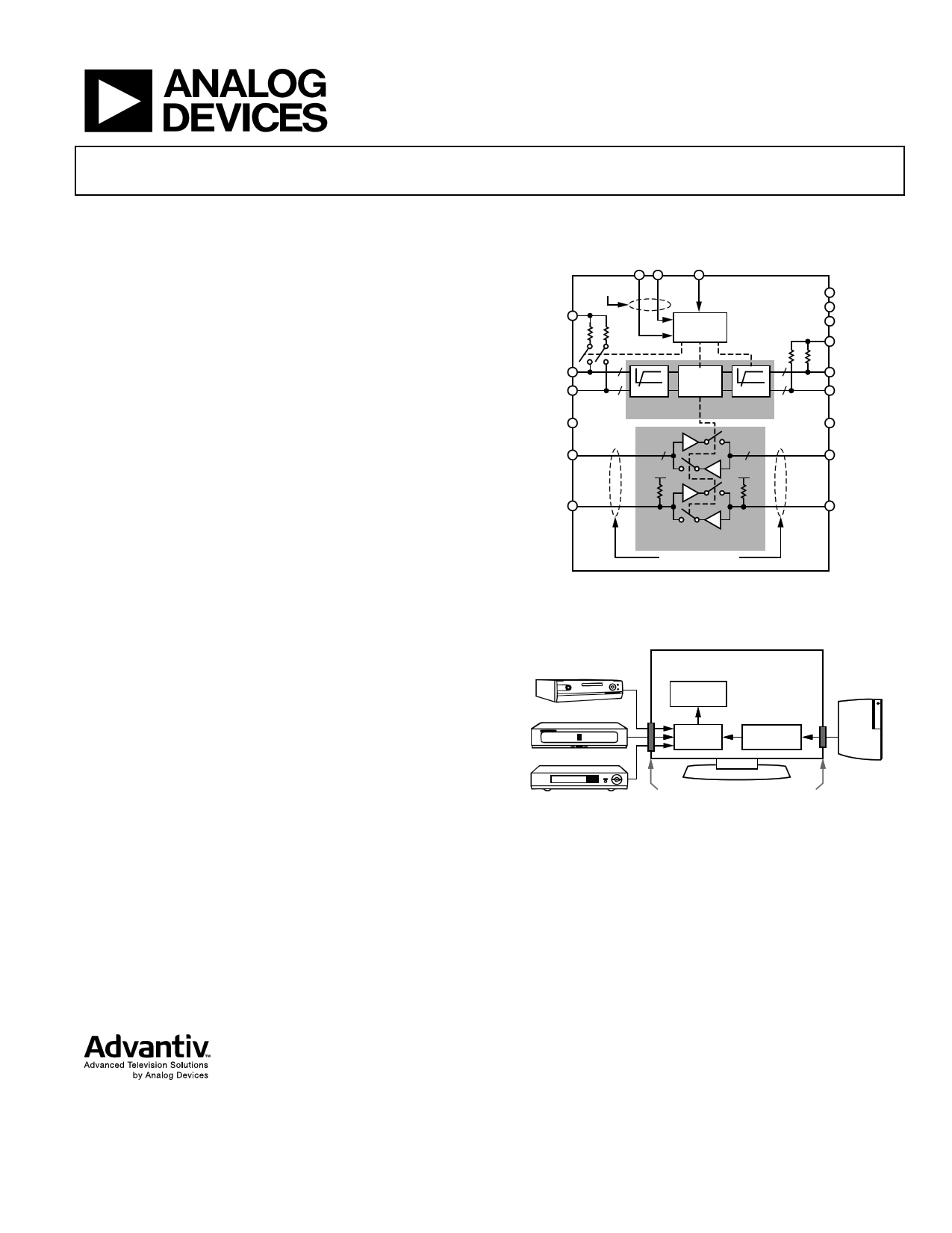
FUNCTIONAL BLOCK DIAGRAM
PARALLEL
VTTI
CONTROL
LOGIC
AD8195
AVCC
AMUXVCC
AVEE
VTTO
IP[3:0]
IN[3:0]
+
–
VREF_IN
44
4 EQ BUFFER PE 4
HIGH SPEED BUFFERED
+ OP[3:0]
– ON[3:0]
VREF_OUT
SCL_IN
SDA_IN
22
SCL_OUT
SDA_OUT
CEC_IN
LOW SPEED BUFFERED
BIDIRECTIONAL
Figure 1.
CEC_OUT
TYPICAL APPLICATION
MEDIA CENTER
SET-TOP BOX
DVD PLAYER
HDMI
RECEIVER
4:1 HDMI
SWITCH
HDTV SET
AD8195
GAME
CONSOLE
BACK PANEL
CONNECTORS
FRONT PANEL
CONNECTOR
Figure 2. Typical AD8195 Application for HDTV Sets
PRODUCT HIGHLIGHTS
1. Enables a fully HDMI 1.3a-compliant front panel input.
2. Supports data rates of up to 2.25 Gbps, enabling 1080p deep
color (12-bit color) HDMI formats and greater than UXGA
(1600 × 1200) DVI resolutions.
3. Input cable equalizer enables use of long cables; more than
20 meters (24 AWG) at data rates of up to 2.25 Gbps.
4. Auxiliary buffer isolates and buffers the DDC bus and CEC
line for a single chip, fully HDMI 1.3a-compliant solution.
5. Auxiliary buffer is powered independently from the TMDS
link so that DDC/CEC functionality can be maintained
when the system is powered off.
One Technology Way, P.O. Box 9106, Norwood, MA 02062-9106, U.S.A.
Tel: 781.329.4700
www.analog.com
Fax: 781.461.3113 ©2008–2012 Analog Devices, Inc. All rights reserved.
1 page 
AD8195
Data Sheet
AUXILIARY CHANNEL PERFORMANCE SPECIFICATIONS
Table 2.
Parameter
DDC CHANNELS
Input Capacitance, CAUX
Input Low Voltage, VIL
Input High Voltage, VIH
Output Low Voltage, VOL
Output High Voltage, VOH
Rise Time
Fall Time
Leakage
CEC CHANNEL
Input Capacitance, CAUX
Input Low Voltage, VIL
Input High Voltage, VIH
Output Low Voltage, VOL
Output High Voltage, VOH
Rise Time
Fall Time
Pull-Up Resistance
Leakage
Test Conditions/Comments
DC bias = 2.5 V, ac voltage = 3.5 V p-p, f = 100 kHz
IOL = 5 mA
10% to 90%, no load
90% to 10%, CLOAD = 400 pF
Input voltage = 5.0 V
DC bias = 1.65 V, ac voltage = 2.5 V p-p, f = 100 kHz,
2 kΩ pull-up resistor from CEC_OUT to 3.3 V
10% to 90%, CLOAD = 1500 pF, RPULL-UP = 27 kΩ;
or CLOAD = 7200 pF, RPULL-UP = 3 kΩ
90% to 10%, CLOAD = 1500pF, RPULL-UP = 27 kΩ;
or CLOAD = 7200 pF, RPULL-UP = 3 kΩ
Off leakage test conditions2
Min
0.7 × VREF1
2.0
2.5
Typ Max Unit
10
0.25
VREF1
140
100
15
0.5
VREF1
0.4
200
10
pF
V
V
V
V
ns
ns
μA
5 25
0.8
0.25 0.6
3.3
50 100
5 10
27
1.8
pF
V
V
V
V
µs
µs
kΩ
µA
1 VREF is the voltage at the reference pin (VREF_IN for SCL_IN and SDA_IN, or VREF_OUT for SCL_OUT and SDA_OUT); nominally 5.0 V.
2 Off leakage test conditions are described in the HDMI Compliance Test Specification 1.3b Section 8, Test ID 8-14: “Remove power (mains) from DUT. Connect CEC line
to 3.63 V via 27 kΩ ± 5% resistor with ammeter in series. Measure CEC line leakage.”
POWER SUPPLY AND CONTROL LOGIC SPECIFICATIONS
Table 3.
Parameter
POWER SUPPLY
AVCC
AMUXVCC
VREF_IN, VREF_OUT
QUIESCENT CURRENT
AVCC
VTTI
VTTO
VREF_IN
VREF_OUT
AMUXVCC
POWER DISSIPATION
PARALLEL CONTROL INTERFACE
Input High Voltage, VIH
Input Low Voltage, VIL
Test Conditions/Comments
Operating range (3.3 V ± 10%)
Operating range (5 V ± 10%)
Output disabled
Output enabled, no preemphasis (0 dB)
Output enabled, maximum preemphasis (6 dB)
Input termination on
Output termination on, no preemphasis
Output termination on, maximum preemphasis
Output disabled
Output enabled, no preemphasis (0 dB)
Output enabled, maximum preemphasis (6 dB)
TX_EN, PE_EN
Rev. B | Page 4 of 20
Min Typ Max Unit
3 3.3 3.6
4.5 5
5.5
3 5.5
V
V
V
20 40
32 50
66 80
40 54
40 50
80 100
120 200
120 200
10 20
mA
mA
mA
mA
mA
mA
μA
μA
mA
116 254 mW
180 663 mW
736 1047 mW
2.4 V
0.8 V
5 Page 
AD8195
Data Sheet
TA = 27°C, AVCC = 3.3 V, VTTI = 3.3 V, VTTO = 3.3 V, AVEE = 0 V, differential input swing = 1000 mV, pattern = PRBS 27 − 1,
TMDS outputs terminated with external 50 Ω resistors to 3.3 V, unless otherwise noted.
HDMI CABLE
DIGITAL
PATTERN
GENERATOR
AD8195
EVALUATION
BOARD
SERIAL DATA
ANALYZER
REFERENCE EYE DIAGRAM AT TP1
SMA COAX CABLE
TP1 TP2
Figure 13. Test Circuit Diagram for Tx Eye Diagrams
TP3
0.125UI/DIV AT 2.25Gbps
Figure 14. Tx Eye Diagram at TP2, PE = 0 dB, Data Rate = 2.25 Gbps
0.125UI/DIV AT 2.25Gbps
Figure 16. Tx Eye Diagram at TP3, PE = 0 dB, Data Rate = 2.25 Gbps
(Cable = 6 Meters, 24 AWG)
0.167UI/DIV AT 3.0Gbps
Figure 15. Tx Eye Diagram at TP2, PE = 0 dB, Data Rate = 3.0 Gbps
0.167UI/DIV AT 3.0Gbps
Figure 17. Tx Eye Diagram at TP3, PE = 0 dB, Data Rate = 3.0 Gbps
(Cable = 6 Meters, 24 AWG)
Rev. B | Page 10 of 20
11 Page | ||
| Páginas | Total 21 Páginas | |
| PDF Descargar | [ Datasheet AD8195.PDF ] | |
Hoja de datos destacado
| Número de pieza | Descripción | Fabricantes |
| AD8190 | 2:1 HDMI/DVI Switch | Analog Devices |
| AD8191 | HDMI/DVI Switch | Analog Devices |
| AD8192 | 2:1 HDMI/DVI Switch | Analog Devices |
| AD8193 | Buffered 2:1 TMDS Switch | Analog Devices |
| Número de pieza | Descripción | Fabricantes |
| SLA6805M | High Voltage 3 phase Motor Driver IC. |
Sanken |
| SDC1742 | 12- and 14-Bit Hybrid Synchro / Resolver-to-Digital Converters. |
Analog Devices |
|
DataSheet.es es una pagina web que funciona como un repositorio de manuales o hoja de datos de muchos de los productos más populares, |
| DataSheet.es | 2020 | Privacy Policy | Contacto | Buscar |