|
|
|
PDF ADIS16367 Data sheet ( Hoja de datos )
| Número de pieza | ADIS16367 | |
| Descripción | Six Degrees of Freedom Inertial Sensor | |
| Fabricantes | Analog Devices | |
| Logotipo | ||
Hay una vista previa y un enlace de descarga de ADIS16367 (archivo pdf) en la parte inferior de esta página. Total 21 Páginas | ||
|
No Preview Available !
Data Sheet
Six Degrees of Freedom Inertial Sensor
ADIS16367
FEATURES
GENERAL DESCRIPTION
Tri-axis digital gyroscope with digital range scaling
±300°/sec, ±600°/sec, ±1200°/sec settings
Tight orthogonal alignment: 0.05°
Tri-axis digital accelerometer: ±18 g
Autonomous operation and data collection
No external configuration commands required
Start-up time: 180 ms
Sleep mode recovery time: 4 ms
Factory-calibrated sensitivity, bias, and axial alignment
Calibration temperature range: −40°C to +85°C
SPI-compatible serial interface
Wide bandwidth: 330 Hz
Embedded temperature sensor
Programmable operation and control
Automatic and manual bias correction controls
Bartlett window, FIR filter length, number of taps
Digital I/O: data ready, alarm indicator, general-purpose
Alarms for condition monitoring
Sleep mode for power management
The ADIS16367 iSensor® is a complete inertial system that includes
a tri-axis gyroscope and tri-axis accelerometer. Each sensor in
the ADIS16367 combines industry-leading iMEMS® technology
with signal conditioning that optimizes dynamic performance.
The factory calibration characterizes each sensor for sensitivity,
bias, alignment, and linear acceleration (gyro bias). As a result, each
sensor has its own dynamic compensation formulas that provide
accurate sensor measurements over a temperature range of
−40°C to +85°C.
The ADIS16367 provides a simple, cost-effective method for
integrating accurate, multiaxis inertial sensing into industrial
systems, especially when compared with the complexity and
investment associated with discrete designs. All necessary motion
testing and calibration are part of the production process at the
factory, greatly reducing system integration time. Tight orthogonal
alignment simplifies inertial frame alignment in navigation
systems. An improved SPI interface and register structure provide
faster data collection and configuration control.
DAC output voltage
Enable external sample clock input: up to 1.2 kHz
Single-command self-test
Single-supply operation: 4.75 V to 5.25 V
2000 g shock survivability
Operating temperature range: −40°C to +105°C
APPLICATIONS
The ADIS16367 uses a compatible pinout and the same package
as the ADIS1635x family. Therefore, systems that currently use
the ADIS1635x family can upgrade their performance with minor
firmware adjustments in their processor designs.
This compact module is approximately 23 mm × 23 mm × 23 mm
and provides a flexible connector interface that enables multiple
mounting orientation options.
Medical instrumentation
Robotics
Platform controls
Navigation
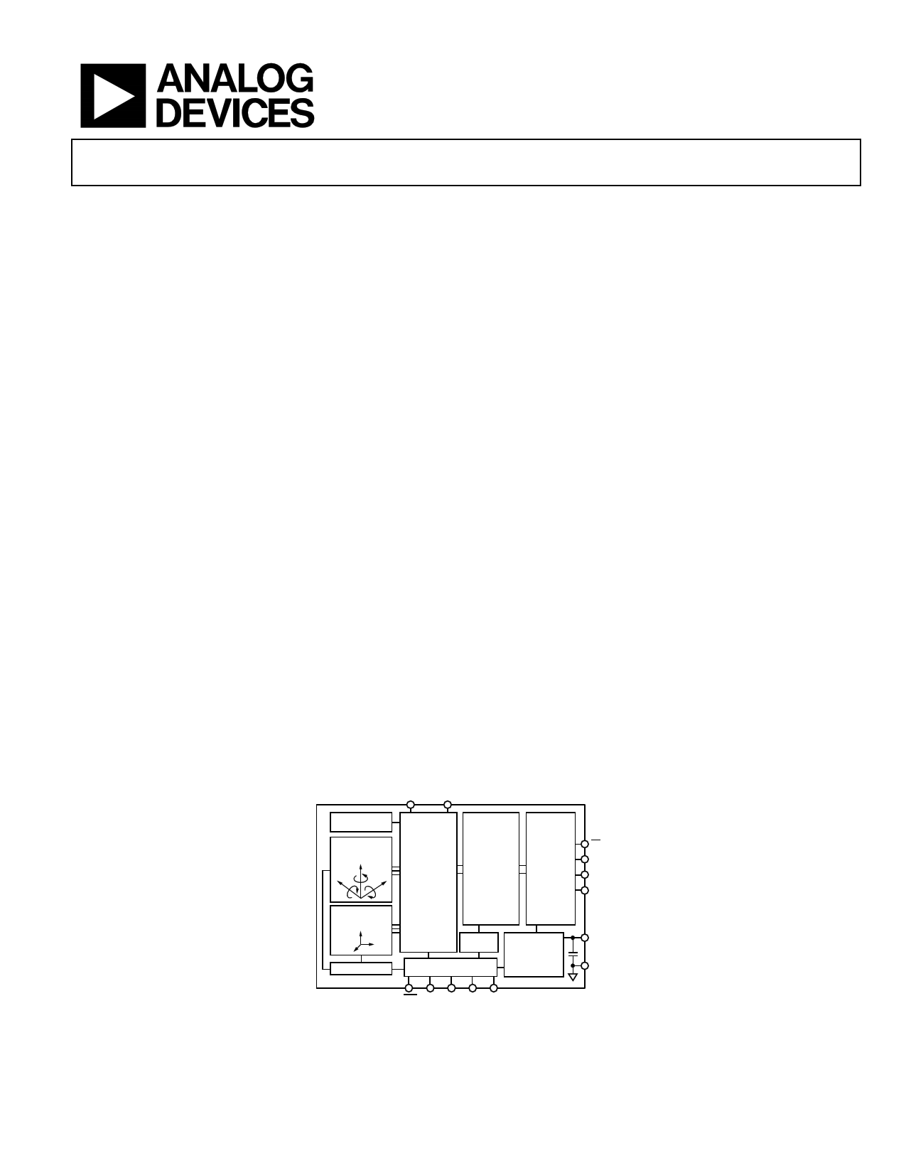
FUNCTIONAL BLOCK DIAGRAM
AUX_
ADC
AUX_
DAC
TEMPERATURE
SENSOR
MEMS
ANGULAR RATE
SENSOR
SIGNAL
CONDITIONING
AND
CONVERSION
CALIBRATION
AND
DIGITAL
PROCESSING
OUTPUT
REGISTERS
AND SPI
INTERFACE
CS
SCLK
DIN
DOUT
TRI-AXIS MEMS
ACCELERATION
SENSOR
SELF-TEST
ADIS16367
ALARMS
DIGITAL
CONTROL
POWER
MANAGEMENT
RST DIO1 DIO2 DIO3 DIO4/
CLKIN
Figure 1.
VCC
GND
Rev. B
Information furnished by Analog Devices is believed to be accurate and reliable. However, no
responsibilityisassumedbyAnalogDevices for itsuse,nor foranyinfringementsofpatentsor other
rights of third parties that may result from its use. Specifications subject to change without notice. No
license is granted by implication or otherwise under any patent or patent rights of Analog Devices.
Trademarksandregisteredtrademarksarethepropertyoftheirrespectiveowners.
One Technology Way, P.O. Box 9106, Norwood, MA 02062-9106, U.S.A.
Tel: 781.329.4700
www.analog.com
Fax: 781.461.3113 ©2010–2012 Analog Devices, Inc. All rights reserved.
1 page 
ADIS16367
Data Sheet
Parameter
DAC OUTPUT
Resolution
Relative Accuracy
Differential Nonlinearity
Offset Error
Gain Error
Output Range
Output Impedance
Output Settling Time
LOGIC INPUTS1
Input High Voltage, VIH
Input Low Voltage, VIL
CS Wake-Up Pulse Width
Logic 1 Input Current, IIH
Logic 0 Input Current, IIL
All Pins Except RST
RST Pin
Input Capacitance, CIN
DIGITAL OUTPUTS1
Output High Voltage, VOH
Output Low Voltage, VOL
FLASH MEMORY
Data Retention3
FUNCTIONAL TIMES4
Power-On, Start-Up Time
Reset Recovery Time
Sleep Mode Recovery Time
Flash Memory Test Time
Automatic Self-Test Time
CONVERSION RATE
Clock Accuracy
Sync Input Clock5
POWER SUPPLY
Power Supply Current
Test Conditions/Comments
5 kΩ/100 pF to GND
101 LSB ≤ input code ≤ 4095 LSB
CS signal to wake up from sleep mode
VIH = 3.3 V
VIL = 0 V
ISOURCE = 1.6 mA
ISINK = 1.6 mA
Endurance2
TJ = 85°C
Time until data is available
Normal mode, SMPL_PRD ≤ 0x09
Low power mode, SMPL_PRD ≥ 0x0A
Normal mode, SMPL_PRD ≤ 0x09
Low power mode, SMPL_PRD ≥ 0x0A
Normal mode, SMPL_PRD ≤ 0x09
Low power mode, SMPL_PRD ≥ 0x0A
Normal mode, SMPL_PRD ≤ 0x09
Low power mode, SMPL_PRD ≥ 0x0A
SMPL_PRD = 0x0001
SMPL_PRD = 0x0001 to 0x00FF
Operating voltage range, VCC
Low power mode
Normal mode
Sleep mode
Min Typ
12
±4
±1
±5
±0.5
0
2
10
2.0
20
±0.2
40
1
10
2.4
10,000
20
0.413
180
250
60
130
4
9
17
90
12
0.8
4.75 5.0
24
49
500
Max Unit
Bits
LSB
LSB
mV
%
3.3 V
Ω
µs
V
0.8 V
0.55 V
µs
±10 µA
60 µA
mA
pF
V
0.4 V
Cycles
Years
819.2
±3
1.2
5.25
ms
ms
ms
ms
ms
ms
ms
ms
ms
SPS
%
kHz
V
mA
mA
µA
1 The digital I/O signals are driven by an internal 3.3 V supply, and the inputs are 5 V tolerant.
2 Endurance is qualified as per JEDEC Standard 22, Method A117, and measured at −40°C, +25°C, +85°C, and +125°C.
3 The data retention lifetime equivalent is at a junction temperature (TJ) of 85°C as per JEDEC Standard 22, Method A117. Data retention lifetime decreases with junction
temperature.
4 These times do not include thermal settling and internal filter response times (330 Hz bandwidth), which may affect overall accuracy.
5 The sync input clock functions below the specified minimum value, at reduced performance levels.
Rev. B | Page 4 of 20
5 Page 
ADIS16367
Data Sheet
MEMORY MAP
Table 8. User Register Memory Map
Name
User Access Flash Backup
FLASH_CNT Read only
Yes
SUPPLY_OUT Read only
No
XGYRO_OUT Read only
No
YGYRO_OUT Read only
No
ZGYRO_OUT Read only
No
XACCL_OUT Read only
No
YACCL_OUT Read only
No
ZACCL_OUT Read only
No
XTEMP_OUT Read only
No
YTEMP_OUT Read only
No
ZTEMP_OUT Read only
No
AUX_ADC
Read only
No
Reserved
N/A
N/A
XGYRO_OFF Read/write Yes
YGYRO_OFF Read/write Yes
ZGYRO_OFF Read/write Yes
XACCL_OFF Read/write Yes
YACCL_OFF Read/write Yes
ZACCL_OFF Read/write Yes
ALM_MAG1 Read/write Yes
ALM_MAG2 Read/write Yes
ALM_SMPL1 Read/write Yes
ALM_SMPL2 Read/write Yes
ALM_CTRL
Read/write Yes
AUX_DAC
Read/write No
GPIO_CTRL Read/write No
MSC_CTRL
Read/write Yes
SMPL_PRD
Read/write Yes
SENS_AVG
Read/write Yes
SLP_CNT
Write only
No
DIAG_STAT
Read only
No
GLOB_CMD Write only
N/A
Reserved
N/A
N/A
LOT_ID1
Read only
Yes
LOT_ID2
Read only
Yes
PROD_ID
Read only
Yes
SERIAL_NUM Read only
Yes
Address1
0x00
0x02
0x04
0x06
0x08
0x0A
0x0C
0x0E
0x10
0x12
0x14
0x16
0x18
0x1A
0x1C
0x1E
0x20
0x22
0x24
0x26
0x28
0x2A
0x2C
0x2E
0x30
0x32
0x34
0x36
0x38
0x3A
0x3C
0x3E
0x40 to 0x51
0x52
0x54
0x56
0x58
Default
N/A
N/A
N/A
N/A
N/A
N/A
N/A
N/A
N/A
N/A
N/A
N/A
N/A
0x0000
0x0000
0x0000
0x0000
0x0000
0x0000
0x0000
0x0000
0x0000
0x0000
0x0000
0x0000
0x0000
0x0006
0x0001
0x0402
0x0000
0x0000
0x0000
N/A
N/A
N/A
0x3FEF
N/A
Register Description
Flash memory write count
Power supply measurement
X-axis gyroscope output
Y-axis gyroscope output
Z-axis gyroscope output
X-axis accelerometer output
Y-axis accelerometer output
Z-axis accelerometer output
X-axis gyroscope temperature output
Y-axis gyroscope temperature output
Z-axis gyroscope temperature output
Auxiliary ADC output
Reserved
X-axis gyroscope bias offset factor
Y-axis gyroscope bias offset factor
Z-axis gyroscope bias offset factor
X-axis acceleration bias offset factor
Y-axis acceleration bias offset factor
Z-axis acceleration bias offset factor
Alarm 1 amplitude threshold
Alarm 2 amplitude threshold
Alarm 1 sample size
Alarm 2 sample size
Alarm control
Auxiliary DAC data
Auxiliary digital input/output control
Data-ready, self-test, miscellaneous
Internal sample period (rate) control
Dynamic range and digital filter control
Sleep mode control
System status
System command
Reserved
Lot Identification Code 1
Lot Identification Code 2
Product identification
Serial number
Bit Function
N/A
See Table 9
See Table 9
See Table 9
See Table 9
See Table 9
See Table 9
See Table 9
See Table 9
See Table 9
See Table 9
See Table 9
N/A
See Table 15
See Table 15
See Table 15
See Table 16
See Table 16
See Table 16
See Table 27
See Table 27
See Table 28
See Table 28
See Table 29
See Table 23
See Table 21
See Table 22
See Table 18
See Table 20
See Table 19
See Table 26
See Table 17
N/A
See Table 32
See Table 32
See Table 32
See Table 32
1 Each register contains two bytes. The address of the lower byte is displayed. The address of the upper byte is equal to the address of the lower byte plus 1.
Rev. B | Page 10 of 20
11 Page | ||
| Páginas | Total 21 Páginas | |
| PDF Descargar | [ Datasheet ADIS16367.PDF ] | |
Hoja de datos destacado
| Número de pieza | Descripción | Fabricantes |
| ADIS16360 | Six Degrees of Freedom Inertial Sensor | Analog Devices |
| ADIS16362 | Six Degrees of Freedom Inertial Sensor | Analog Devices |
| ADIS16364 | Six Degrees of Freedom Inertial Sensor | Analog Devices |
| ADIS16365 | Tri-Axis Inertial Sensor | Analog Devices |
| Número de pieza | Descripción | Fabricantes |
| SLA6805M | High Voltage 3 phase Motor Driver IC. |
Sanken |
| SDC1742 | 12- and 14-Bit Hybrid Synchro / Resolver-to-Digital Converters. |
Analog Devices |
|
DataSheet.es es una pagina web que funciona como un repositorio de manuales o hoja de datos de muchos de los productos más populares, |
| DataSheet.es | 2020 | Privacy Policy | Contacto | Buscar |