|
|
|
PDF ADuM225N Data sheet ( Hoja de datos )
| Número de pieza | ADuM225N | |
| Descripción | 5.0 kV RMS Dual Channel Digital Isolators | |
| Fabricantes | Analog Devices | |
| Logotipo | ||
Hay una vista previa y un enlace de descarga de ADuM225N (archivo pdf) en la parte inferior de esta página. Total 23 Páginas | ||
|
No Preview Available !
Data Sheet
5.0 kV RMS Dual Channel Digital Isolators
ADuM220N/ADuM221N/ADuM225N/ADuM226N
FEATURES
High common-mode transient immunity: 100 kV/μs
High robustness to radiated and conducted noise
Low propagation delay: 13 ns maximum for 5 V operation,
15 ns maximum for 1.8 V operation
150 Mbps maximum data rate
Safety and regulatory approvals (pending)
UL recognition: 5000 V rms for 1 minute per UL 1577
CSA Component Acceptance Notice 5A
VDE certificate of conformity
DIN V VDE V 0884-10 (VDE V 0884-10):2006-12
VIORM = 849 V peak
10,000 V peak surge/impulse voltage rating
CQC Certification per GB4943.1-2011
Low dynamic power consumption
1.8 V to 5 V level translation
High temperature operation: 125°C maximum
Fail-safe high or low options
8-lead/16-lead, RoHS compliant SOIC packages
Qualified for automotive applications
APPLICATIONS
General-purpose multichannel isolation
Industrial field bus isolation
Automotive systems
GENERAL DESCRIPTION
The ADuM220N/ADuM221N/ADuM225N/ADuM226N1 are
dual-channel digital isolators based on Analog Devices, Inc.,
iCoupler® technology. Combining high speed, complementary
metal-oxide semiconductor (CMOS) and monolithic air core
transformer technology, these isolation components provide
outstanding performance characteristics superior to alternatives
such as optocoupler devices and other integrated couplers. The
maximum propagation delay is 13 ns with a pulse width distortion
(PWD) of less than 3 ns at 5 V operation. Channel matching is
tight at 3.0 ns maximum.
The ADuM220N/ADuM221N/ADuM225N/ADuM226N data
channels are independent and are available in a variety of
configurations with a withstand voltage rating of 5.0 kV rms (see
the Ordering Guide). The devices operate with the supply voltage
on either side ranging from 1.8 V to 5 V, providing compatibil-
ity with lower voltage systems as well as enabling voltage translation
functionality across the isolation barrier. Unlike other optocoupler
alternatives, dc correctness is ensured in the absence of input logic
transitions. Two different fail-safe options are available, in which
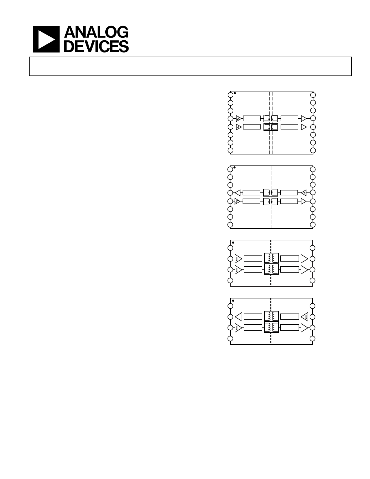
FUNCTIONAL BLOCK DIAGRAMS
GND1 1
NIC 2
VDD1 3
VIA 4
VIB 5
NIC 6
GND1 7
NIC 8
ENCODE
ENCODE
ADuM220N 16 GND2
15 NIC
DECODE
14 VDD2
13 VOA
DECODE
12 VOB
11 NIC
10 NIC
Figure 1.
9 GND2
GND1 1
NIC 2
VDD1 3
VOA 4
VIB 5
NIC 6
GND1 7
NIC 8
DECODE
ENCODE
ADuM221N
ENCODE
DECODE
Figure 2.
16 GND2
15 NIC
14 VDD2
13 VIA
12 VOB
11 NIC
10 NIC
9 GND2
VDD1 1
ADuM225N
8 VDD2
VIA 2
ENCODE
DECODE
7 VOA
VIB 3
ENCODE
DECODE
6 VOB
GND1 4
Figure 3.
5 GND2
VDD1 1
ADuM226N
8 VDD2
VOA 2
DECODE
ENCODE
7 VIA
VIB 3
ENCODE
DECODE
6 VOB
GND1 4
5 GND2
Figure 4
the outputs transition to a predetermined state when the input
power supply is not applied or the inputs are disabled.The
ADuM220N0 is pin compatible with the ADuM2210 RW-16
package. The ADuM220N1 is pin compatible with the
ADuM2200 RW-16 package. The ADuM221N0 is pin compati-
ble with the ADuM2211 RW-16 package. The ADuM221N1 is
pin compatible with the ADuM2201 RW-16 package.
1 Protected by U.S. Patents 5,952,849; 6,873,065; 6,903,578; and 7,075,329. Other patents are pending.
Rev. A
Document Feedback
Information furnished by Analog Devices is believed to be accurate and reliable. However, no
responsibility is assumed by Analog Devices for its use, nor for any infringements of patents or other
rights of third parties that may result from its use. Specifications subject to change without notice. No
license is granted by implication or otherwise under any patent or patent rights of Analog Devices.
Trademarksandregisteredtrademarksarethepropertyoftheirrespectiveowners.
One Technology Way, P.O. Box 9106, Norwood, MA 02062-9106, U.S.A.
Tel: 781.329.4700
©2016 Analog Devices, Inc. All rights reserved.
Technical Support
www.analog.com
1 page 
Data Sheet
ADuM220N/ADuM221N/ADuM225N/ADuM226N
Parameter
Output Voltage
Logic High
Logic Low
Input Current per Channel
Quiescent Supply Current
ADuM220N/ADuM225N
ADuM221N/ADuM226N
Dynamic Supply Current
Dynamic Input
Dynamic Output
Undervoltage Lockout
Positive VDDx Threshold
Negative VDDx Threshold
VDDx Hysteresis
AC SPECIFICATIONS
Output Rise/Fall Time
Common-Mode Transient
Immunity6
Symbol Min Typ Max
VOH VDDx − 0.1 VDDx
VDDx − 0.4 VDDx − 0.2
VOL 0.0 0.1
0.2 0.4
II
−10
+0.01
+10
IDD1 (Q)
IDD2 (Q)
IDD1 (Q)
IDD2 (Q)
IDD1 (Q)
IDD2 (Q)
IDD1 (Q)
IDD2 (Q)
IDDI (D)
IDDO (D)
UVLO
VDDxUV+
VDDxUV−
VDDxUVH
tR/tF
|CMH|
|CML|
75
75
0.8 1.3
1.2 1.8
6.3 9.7
1.3 1.8
1.0 1.6
1.0 1.5
3.9 5.8
4.8 6.4
0.01
0.01
1.6
1.5
0.1
2.5
100
100
Unit
V
V
V
V
µA
Test Conditions/Comments
IOx1 = −20 µA, VIx = VIxH2
IOx1 = −2 mA, VIx = VIxH2
IOx1 = 20 µA, VIx = VIxL3
IOx1 = 2 mA, VIx = VIxL3
0 V ≤ VIx ≤ VDDx
mA VI4 = 0 (N0), 1 (N1)5
mA VI4 = 0 (N0), 1 (N1)5
mA VI4 = 1 (N0), 0 (N1)5
mA VI4 = 1 (N0), 0 (N1)5
mA
mA
mA
mA
mA/Mbps
mA/Mbps
VI4 = 0 (N0), 1 (N1)5
VI4 = 0 (N0), 1 (N1)5
VI4 = 1 (N0), 0 (N1)5
VI4 = 1 (N0), 0 (N1)5
Inputs switching, 50% duty cycle
V
V
V
ns
kV/µs
kV/µs
10% to 90%
VIx = VDDx, VCM = 1000 V, transient
magnitude = 800 V
VIx = 0 V, VCM = 1000 V, transient
magnitude = 800 V
1 IOx is the Channel x output current, where x is A or B.
2 VIxH is the input side logic high.
3 VIxL is the input side logic low.
4 VI is the voltage input.
5 N0 refers to the ADuM220N0/ADuM221N0/ADuM225N0/ADuM226N0 models, and N1 refers to the ADuM220N1/ADuM221N1/ADuM225N1/ADuM226N1 models. See
the Ordering Guide section.
6 |CMH| is the maximum common-mode voltage slew rate that can be sustained while maintaining VO > 0.8 VDDx. |CML| is the maximum common-mode voltage slew rate
that can be sustained while maintaining VO > 0.8 V. The common-mode voltage slew rates apply to both rising and falling common-mode voltage edges.
Table 4. Total Supply Current vs. Data Throughput
1 Mbps
Parameter
Symbol
Min Typ Max
SUPPLY CURRENT
ADuM220N/ADuM225N
Supply Current Side 1
IDD1
3.6 6.2
Supply Current Side 2
IDD2
1.3 1.9
ADuM221N/ADuM226N
Supply Current Side 1
IDD1
2.5 4.6
Supply Current Side 2
IDD2
2.9 4.8
25 Mbps
Min Typ Max
4.0 6.7
2.1 3.1
3.0 5.5
3.5 5.8
100 Mbps
Min Typ Max
5.6 9.1
4.4 6.8
5.0 8.1
5.4 8.3
Unit
mA
mA
mA
mA
Rev. A | Page 5 of 23
5 Page 
Data Sheet
ADuM220N/ADuM221N/ADuM225N/ADuM226N
DIN V VDE V 0884-10 (VDE V 0884-10) INSULATION CHARACTERISTICS
These ADuM220N/ADuM221N/ADuM225N/ADuM226N isolators are suitable for reinforced electrical isolation only within the safety
limit data. Protective circuits ensure the maintenance of the safety data. The * marking on packages denotes DIN V VDE V 0884-10
approval.
Table 15.
Description
Installation Classification per DIN VDE 0110
For Rated Mains Voltage ≤ 150 V rms
For Rated Mains Voltage ≤ 300 V rms
For Rated Mains Voltage ≤ 600 V rms
Climatic Classification
Pollution Degree per DIN VDE 0110, Table 1
Maximum Working Insulation Voltage
Input to Output Test Voltage, Method B1
Input to Output Test Voltage, Method A
After Environmental Tests Subgroup 1
After Input and/or Safety Test Subgroup 2
and Subgroup 3
Highest Allowable Overvoltage
Surge Isolation Voltage Basic
Surge Isolation Voltage Reinforced
Safety Limiting Values
Maximum Junction Temperature
Total Power Dissipation at 25°C
ADuM220N/ADuM221N
ADuM225N/ADuM226N
Insulation Resistance at TS
Test Conditions/Comments
VIORM × 1.875 = Vpd (m), 100% production test,
tini = tm = 1 sec, partial discharge < 5 pC
VIORM × 1.5 = Vpd (m), tini = 60 sec, tm = 10 sec,
partial discharge < 5 pC
VIORM × 1.2 = Vpd (m), tini = 60 sec, tm = 10 sec,
partial discharge < 5 pC
VPEAK = 16 kV, 1.2 µs rise time, 50 µs,
50% fall time
VPEAK = 16 kV, 1.2 µs rise time, 50 µs,
50% fall time
Maximum value allowed in the event of a
failure (see Figure 5 or Figure 6)
VIO = 500 V
Symbol Characteristic Unit
VIORM
Vpd (m)
I to IV
I to IV
I to IV
40/105/21
2
849
1592
V peak
V peak
Vpd (m)
VIOTM
VIOSM
VIOSM
1274
1019
7000
16,000
10,000
V peak
V peak
V peak
V peak
V peak
TS 150
PS
2.78
1.56
RS >109
°C
W
W
Ω
3.0
2.5
2.0
1.5
1.0
0.5
0
0 50 100 150 200
AMBIENT TEMPERATURE (°C)
Figure 5. ADuM220N/ADuM221N Thermal Derating Curve, Dependence of
Safety Limiting Values with Ambient Temperature per DIN V VDE V 0884-10
1.8
1.6
1.4
1.2
1.0
0.8
0.6
0.4
0.2
0
0 50 100 150 200
AMBIENT TEMPERATURE (°C)
Figure 6. ADuM225N/ADuM226N Thermal Derating Curve, Dependence of
Safety Limiting Values with Ambient Temperature per DIN V VDE V 0884-10
Rev. A | Page 11 of 23
11 Page | ||
| Páginas | Total 23 Páginas | |
| PDF Descargar | [ Datasheet ADuM225N.PDF ] | |
Hoja de datos destacado
| Número de pieza | Descripción | Fabricantes |
| ADUM2250 | (ADUM2250 / ADUM2251) Dual I2C Isolators | Analog Devices |
| ADUM2251 | (ADUM2250 / ADUM2251) Dual I2C Isolators | Analog Devices |
| ADuM225N | 5.0 kV RMS Dual Channel Digital Isolators | Analog Devices |
| Número de pieza | Descripción | Fabricantes |
| SLA6805M | High Voltage 3 phase Motor Driver IC. |
Sanken |
| SDC1742 | 12- and 14-Bit Hybrid Synchro / Resolver-to-Digital Converters. |
Analog Devices |
|
DataSheet.es es una pagina web que funciona como un repositorio de manuales o hoja de datos de muchos de los productos más populares, |
| DataSheet.es | 2020 | Privacy Policy | Contacto | Buscar |