|
|
|
PDF ADM2484E Data sheet ( Hoja de datos )
| Número de pieza | ADM2484E | |
| Descripción | Isolated RS-485 Transceiver | |
| Fabricantes | Analog Devices | |
| Logotipo | ||
Hay una vista previa y un enlace de descarga de ADM2484E (archivo pdf) en la parte inferior de esta página. Total 17 Páginas | ||
|
No Preview Available !
Data Sheet
500 kbps, ESD Protected, Half-/Full-Duplex,
iCoupler, Isolated RS-485 Transceiver
ADM2484E
FEATURES
Isolated, RS-485/RS-422 transceiver, configurable as half- or
full-duplex
±15 kV ESD protection on RS-485 input/output pins
500 kbps data rate
Complies with ANSI TIA/EIA RS-485-A-1998 and
ISO 8482: 1987(E)
Suitable for 5 V or 3.3 V operation (VDD1)
High common-mode transient immunity: >25 kV/μs
True fail-safe receiver inputs
256 nodes on the bus
Thermal shutdown protection
Safety and regulatory approvals
UL recognition
5000 V rms isolation voltage for 1 minute per UL1577
VDE certificate of conformity
DIN V VDE V 0884-10 (VDE V 0884-10): 2006-12
Reinforced insulation, VIORM = 849 VPEAK
CSA Component Acceptance Notice 5A
IEC 60950-1: 380 V rms (reinforced)
Operating temperature range: −40°C to +85°C
Wide body, 16-lead SOIC package
APPLICATIONS
Isolated RS-485/RS-422 interfaces
Industrial field networks
INTERBUS
Multipoint data transmission systems
GENERAL DESCRIPTION
The ADM2484E is an isolated data transceiver with ±15 kV
ESD protection suitable for high speed, half- or full-duplex
communication on multipoint transmission lines. For half-
duplex operation, the transmitter outputs and receiver inputs
share the same transmission line. Transmitter Output Pin Y
links externally to Receiver Input Pin A, and Transmitter
Output Pin Z links externally to Receiver Input Pin B.
Designed for balanced transmission lines, the ADM2484E
complies with ANSI TIA/EIA RS-485-A-1998 and ISO 8482:
1987(E). The device employs Analog Devices, Inc., iCoupler®
technology to combine a 3-channel isolator, a three-state
differential line driver, and a differential input receiver into a
single package.
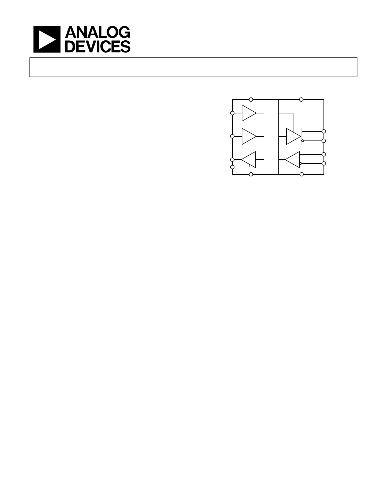
FUNCTIONAL BLOCK DIAGRAM
VDD1
VDD2
ADM2484E
DE
TxD
RxD
RE
GND1
Figure 1.
GND2
Y
Z
A
B
The differential transmitter outputs and receiver inputs feature
electrostatic discharge circuitry that provides protection up to
±15 kV using the human body model (HBM). The logic side of
the device can be powered with either a 5 V or a 3.3 V supply,
whereas the bus side requires an isolated 3.3 V supply.
The device has current-limiting and thermal shutdown features
to protect against output short circuits and situations where bus
contention causes excessive power dissipation.
Rev. F
Document Feedback
Information furnished by Analog Devices is believed to be accurate and reliable. However, no
responsibility is assumed by Analog Devices for its use, nor for any infringements of patents or other
rights of third parties that may result from its use. Specifications subject to change without notice. No
license is granted by implication or otherwise under any patent or patent rights of Analog Devices.
Trademarksandregisteredtrademarksarethepropertyoftheirrespectiveowners.
One Technology Way, P.O. Box 9106, Norwood, MA 02062-9106, U.S.A.
Tel: 781.329.4700 ©2008–2015 Analog Devices, Inc. All rights reserved.
Technical Support
www.analog.com
1 page 
ADM2484E
TIMING SPECIFICATIONS
TA = −40°C to +85°C.
Table 2.
Parameter
DRIVER
Propagation Delay
Differential Driver Output Skew
(tDPLH − tDPHL)
Rise Time/Fall Time
Enable Time
Disable Time
RECEIVER
Propagation Delay
Pulse Width Distortion,
PWD = |tPLH − tPHL|
Enable Time
Disable Time
Data Sheet
Symbol Min Typ Max Unit Test Conditions
tDPLH, tDPHL
tDSKEW
250
700 ns
100 ns
tDR, tDF
tZL, tZH
tLZ, tHZ
200 450 1100 ns
1.5 µs
200 ns
RL = 54 Ω, CL1 = CL2 = 100 pF, see Figure 16 and Figure 21
RL = 54 Ω, CL1 = CL2 = 100 pF, see Figure 16 and Figure 21
RL = 54 Ω, CL1 = CL2 = 100 pF, see Figure 16 and Figure 21
RL = 110 Ω, CL = 50 pF, see Figure 18 and Figure 22
RL = 110 Ω, CL = 50 pF, see Figure 18 and Figure 22
tPLH, tPHL
tPWD
tZL, tZH
tLZ, tHZ
200 ns
30 ns
13 ns
13 ns
CL = 15 pF, see Figure 17 and Figure 23
CL = 15 pF, see Figure 17 and Figure 23
RL = 1 kΩ, CL = 15 pF, see Figure 19 and Figure 24
RL = 1 kΩ, CL = 15 pF, see Figure 19 and Figure 24
PACKAGE CHARACTERISTICS
Table 3.
Parameter
RESISTANCE
Resistance (Input-to-Output)1
CAPACITANCE
Capacitance (Input-to-Output)1
Input Capacitance2
THERMAL RESISTANCE
Input IC Junction-to-Case
Output IC Junction-to-Case
Symbol
RI-O
CI-O
CI
θJCI
θJCO
Min Typ Max Unit Test Conditions
1012 Ω
3 pF f = 1 MHz
4 pF
33 °C/W Thermocouple located at center of package underside
28 °C/W
1 Device considered a 2-terminal device: Pin 1 to Pin 8 are shorted together and Pin 9 to Pin16 are shorted together.
2 Input capacitance is from any input data pin to ground.
REGULATORY INFORMATION
Table 4.
UL1
1577 Component Recognition Program
5000 V rms Isolation Voltage
CSA
Approved under CSA Component Acceptance
Notice 5A
Reinforced insulation per CSA 60950-1-03 and
IEC 60950-1, 380 V rms (537 VPEAK) maximum
working voltage
VDE2
Certified according to DIN V VDE V 0884-10
(VDE V 0884-10): 2006-122
Reinforced insulation, 849 VPEAK
1 In accordance with UL1577, each ADM2484E is proof tested by applying an insulation test voltage ≥ 6000 V rms for 1 second (current leakage detection limit = 10 µA).
2 In accordance with DIN V VDE V 0884-10, each ADM2484E is proof tested by applying an insulation test voltage ≥ 1590 VPEAK for 1 second (partial discharge detection
limit = 5 pC).
Rev. F | Page 4 of 16
5 Page 
ADM2484E
TEST CIRCUITS
VOD
RL
2
RL
2 VOC
Figure 14. Driver Voltage Measurement
375Ω
VOD 60Ω
VTEST
375Ω
Figure 15. Driver Voltage Measurement
Data Sheet
A
VOUT
B CL
Figure 17. Receiver Propagation Delay
0V OR 3V
DE
Y
S1
Z
VOUT
RL
CL
VCC
S2
Figure 18. Driver Enable/Disable
Y CL1
RL
Z CL2
Figure 16. Driver Propagation Delay
+1.5V
–1.5V
S1
RE IN
RL
RE
CL
VOUT
Figure 19. Receiver Enable/Disable
VCC
S2
VDD1
DE
VDD2
VDD2
Y
TxD Z 120Ω
RxD
RE
A
B
GND1
GND2
Figure 20. Supply Current Measurement Test Circuit
Rev. F | Page 10 of 16
11 Page | ||
| Páginas | Total 17 Páginas | |
| PDF Descargar | [ Datasheet ADM2484E.PDF ] | |
Hoja de datos destacado
| Número de pieza | Descripción | Fabricantes |
| ADM2484E | Isolated RS-485 Transceiver | Analog Devices |
| Número de pieza | Descripción | Fabricantes |
| SLA6805M | High Voltage 3 phase Motor Driver IC. |
Sanken |
| SDC1742 | 12- and 14-Bit Hybrid Synchro / Resolver-to-Digital Converters. |
Analog Devices |
|
DataSheet.es es una pagina web que funciona como un repositorio de manuales o hoja de datos de muchos de los productos más populares, |
| DataSheet.es | 2020 | Privacy Policy | Contacto | Buscar |