|
|
|
PDF ADG3241 Data sheet ( Hoja de datos )
| Número de pieza | ADG3241 | |
| Descripción | 2-Port Level Translator Bus Switch | |
| Fabricantes | Analog Devices | |
| Logotipo | ||
Hay una vista previa y un enlace de descarga de ADG3241 (archivo pdf) en la parte inferior de esta página. Total 17 Páginas | ||
|
No Preview Available !
2.5 V/3.3 V, 1-Bit, 2-Port
Level Translator Bus Switch in SOT-66
ADG3241
FEATURES
225 ps propagation delay through the switch
4.5 Ω switch connection between ports
Data rate 1.5 Gbps
2.5 V/3.3 V supply operation
Selectable level shifting/translation
Level translation
3.3 V to 2.5 V
3.3 V to 1.8 V
2.5 V to 1.8 V
Small signal bandwidth 770 MHz
Tiny 6-lead SC70 package and 6-lead SOT-66 package
APPLICATIONS
3.3 V to 1.8 V voltage translation
3.3 V to 2.5 V voltage translation
2.5 V to 1.8 V voltage translation
Bus switching
Bus isolation
Hot swap
Hot plug
Analog switch applications
GENERAL DESCRIPTION
The ADG3241 is a 2.5 V or 3.3 V single digital switch. It is
designed on a low voltage CMOS process that provides low
power dissipation yet gives high switching speed and very low
on resistance. This allows the input to be connected to the
output without additional propagation delay or generating
additional ground bounce noise.
The switch is enabled by means of the bus enable (BE) input
signal. This digital switch allows a bidirectional signal to be
switched when on. In the off condition, signal levels up to the
supplies are blocked.
This device is ideal for applications requiring level translation.
When operated from a 3.3 V supply, level translation from 3.3 V
inputs to 2.5 V outputs is allowed. Similarly, if the device is
operated from a 2.5 V supply and 2.5 V inputs are applied, the
device translates the outputs to 1.8 V. In addition to this, a level
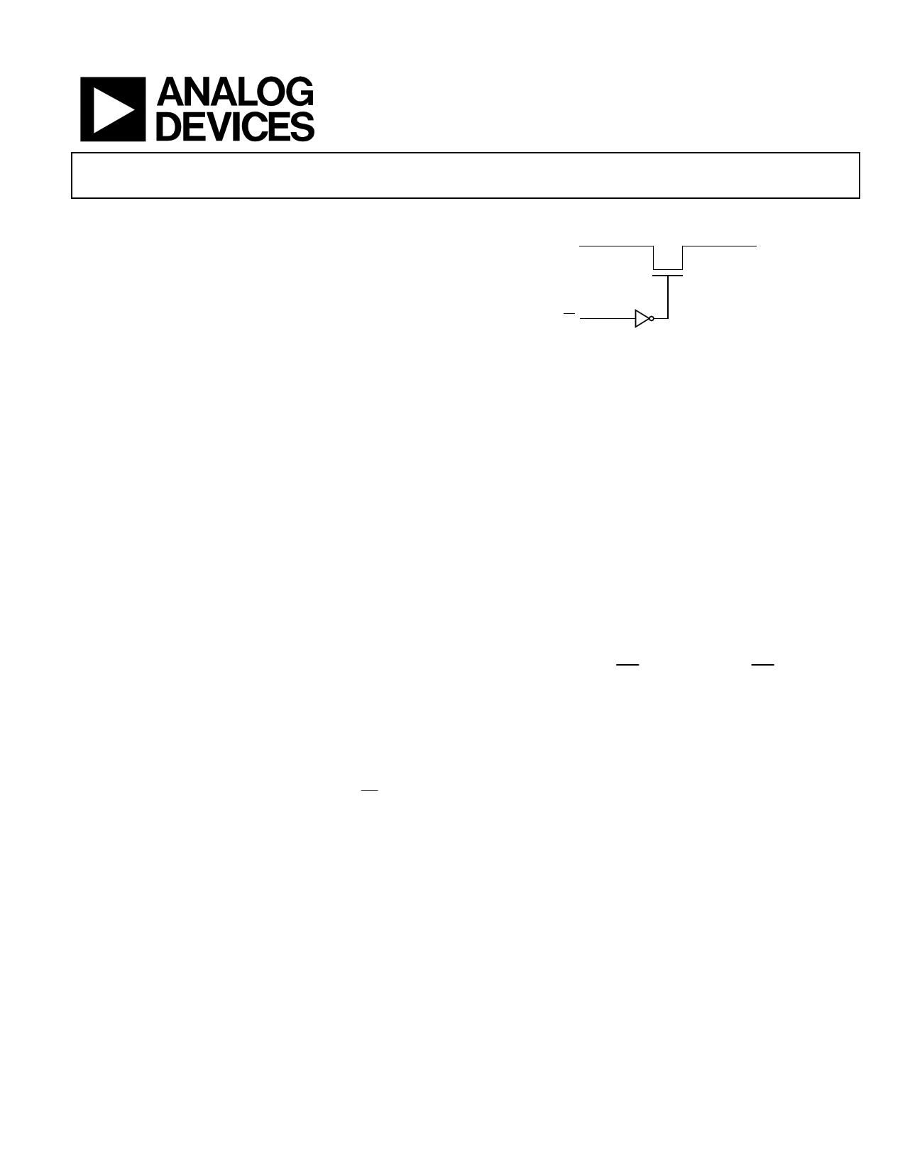
FUNCTIONAL BLOCK DIAGRAM
AB
BE
Figure 1.
translating select pin (SEL) is included. When SEL is low, VCC is
reduced internally, allowing for level translation between 3.3 V
inputs and 1.8 V outputs. This makes the device suited to
applications requiring level translation between different
supplies, such as converter to DSP/microcontroller interfacing.
PRODUCT HIGHLIGHTS
1. 3.3 V or 2.5 V supply operation.
2. Extremely low propagation delay through switch.
3. 4.5 Ω switches connect inputs to outputs.
4. Level and voltage translation.
5. Tiny, SC70 package and SOT-66 package.
Rev. B
Information furnished by Analog Devices is believed to be accurate and reliable. However, no
responsibility is assumed by Analog Devices for its use, nor for any infringements of patents or other
rights of third parties that may result from its use. Specifications subject to change without notice. No
license is granted by implication or otherwise under any patent or patent rights of Analog Devices.
Trademarksandregisteredtrademarksarethepropertyoftheirrespectiveowners.
One Technology Way, P.O. Box 9106, Norwood, MA 02062-9106, U.S.A.
Tel: 781.329.4700
www.analog.com
Fax: 781.461.3113
©2006 Analog Devices, Inc. All rights reserved.
1 page 
ADG3241
ABSOLUTE MAXIMUM RATINGS
TA = 25°C, unless otherwise noted.
Table 2.
Parameter
VCC to GND
Digital Inputs to GND
DC Input Voltage
DC Output Current
Operating Temperature Range
Industrial (B Version)
Storage Temperature Range
Junction Temperature
SC70 Package
θJA Thermal Impedance
SOT-66 Package
θJA Thermal Impedance
Lead Temperature, Soldering (10 sec)
IR Reflow, Peak Temperature
(<20 sec)
Rating
−0.5 V to +4.6 V
−0.5 V to +4.6 V
−0.5 V to +4.6 V
25 mA per channel
−40°C to +85°C
−65°C to +150°C
150°C
332°C/W
191°C/W (4-layer board)
300°C
235°C
Stresses above those listed under Absolute Maximum Ratings
may cause permanent damage to the device. This is a stress
rating only; functional operation of the device at these or any
other conditions above those indicated in the operational
section of this specification is not implied. Exposure to absolute
maximum rating conditions for extended periods may affect
device reliability.
Only one absolute maximum rating can be applied at any one
time.
ESD CAUTION
ESD (electrostatic discharge) sensitive device. Electrostatic charges as high as 4000 V readily accumulate on
the human body and test equipment and can discharge without detection. Although this product features
proprietary ESD protection circuitry, permanent damage may occur on devices subjected to high energy
electrostatic discharges. Therefore, proper ESD precautions are recommended to avoid performance
degradation or loss of functionality.
Rev. B | Page 4 of 16
5 Page 
ADG3241
TERMINOLOGY
VCC
Positive power supply voltage.
GND
Ground (0 V) reference.
VINH
Minimum input voltage for Logic 1.
VINL
Maximum input voltage for Logic 0.
II
Input leakage current at the control inputs.
IOZ
Off state leakage current. It is the maximum leakage current at
the switch pin in the off state.
IOL
On state leakage current. It is the maximum leakage current at
the switch pin in the on state.
VP
Maximum pass voltage. The maximum pass voltage relates to
the clamped output voltage of an NMOS device when the
switch input voltage is equal to the supply voltage.
RON
Ohmic resistance offered by a switch in the on state. It is
measured at a given voltage by forcing a specified amount of
current through the switch.
CX OFF
Off switch capacitance.
CX ON
On switch capacitance.
CIN
Control input capacitance. This consists of BE and SEL.
ICC
Quiescent power supply current. This current represents the
leakage current between the VCC and ground pins. It is
measured when all control inputs are at a logic high or low level
and the switches are off.
ΔICC
Extra power supply current component for the BE control input
when the input is not driven at the supplies.
tPLH, tPHL
Data propagation delay through the switch in the on state.
Propagation delay is related to the RC time constant RON × CL,
where CL is the load capacitance.
tPZH, tPZL
Bus enable times. These are the times taken to cross the VT
voltage at the switch output when the switch turns on in
response to the control signal, BE.
tPHZ, tPLZ
Bus disable times. These are the times taken to place the switch
in the high impedance off state in response to the control signal.
It is measured as the time taken for the output voltage to change
by VΔ from the original quiescent level, with reference to the
logic level transition at the control input. Refer to Figure 26 for
enable and disable times.
Max Data Rate
Maximum rate at which data can be passed through the switch.
Channel Jitter
Peak-to-peak value of the sum of the deterministic and random
jitter of the switch channel.
Rev. B | Page 10 of 16
11 Page | ||
| Páginas | Total 17 Páginas | |
| PDF Descargar | [ Datasheet ADG3241.PDF ] | |
Hoja de datos destacado
| Número de pieza | Descripción | Fabricantes |
| ADG3241 | 2-Port Level Translator Bus Switch | Analog Devices |
| ADG3242 | 2-Bit Common Control Level Translator Bus Switch | Analog Devices |
| ADG3243 | Individual Control Level Translator Bus Switch | Analog Devices |
| ADG3245 | 2.5 V/3.3 V / 8-Bit 2-Port Level Translating / Bus Switch | Analog Devices |
| Número de pieza | Descripción | Fabricantes |
| SLA6805M | High Voltage 3 phase Motor Driver IC. |
Sanken |
| SDC1742 | 12- and 14-Bit Hybrid Synchro / Resolver-to-Digital Converters. |
Analog Devices |
|
DataSheet.es es una pagina web que funciona como un repositorio de manuales o hoja de datos de muchos de los productos más populares, |
| DataSheet.es | 2020 | Privacy Policy | Contacto | Buscar |