|
|
PDF ADT7311 Data sheet ( Hoja de datos )
| Número de pieza | ADT7311 | |
| Descripción | 16-Bit Digital SPI Temperature Sensor | |
| Fabricantes | Analog Devices | |
| Logotipo |  |
|
Hay una vista previa y un enlace de descarga de ADT7311 (archivo pdf) en la parte inferior de esta página. Total 25 Páginas | ||
|
No Preview Available !
Data Sheet
Automotive, ±0.5°C Accurate, 16-Bit
Digital SPI Temperature Sensor
ADT7311
FEATURES
GENERAL DESCRIPTION
Qualified for automotive applications
High performance
Temperature accuracy
±0.5°C from −40°C to +105°C (2.7 V to 3.6 V)
±0.4°C from −40°C to +105°C (3.0 V)
16-bit temperature resolution: 0.0078°C
Fast first conversion on power-up of 6 ms
Easy implementation
No temperature calibration/correction required by user
No linearity correction required
Low power
Power saving 1 sample per second (SPS) mode
700 μW typical at 3.3 V in normal mode
7 μW typical at 3.3 V in shutdown mode
Wide operating ranges
Temperature range: −40°C to +150°C
Voltage range: 2.7 V to 5.5 V
Programmable interrupts
Critical overtemperature interrupt
Overtemperature/undertemperature interrupt
SPI-compatible interface
8-lead narrow SOIC RoHS-compliant package
APPLICATIONS
Battery management
Climate control and infotainment
Lighting
Powertrain
Thermocouple cold junction compensation
GPS
The ADT7311 is a high accuracy digital temperature sensor
in a narrow 8-lead SOIC package. It contains a band gap
temperature reference and a 16-bit ADC to monitor and digitize
the temperature to a 0.0078°C resolution. The ADC resolution,
by default, is set to 13 bits (0.0625°C). The ADC resolution is a
user programmable mode that can be changed through the
serial interface.
The ADT7311 is guaranteed to operate over supply voltages from
2.7 V to 5.5 V. Operating at 3.3 V, the average supply current is
typically 210 μA. The ADT7311 has a shutdown mode that
powers down the device and offers a shutdown current of
typically 2 μA. The ADT7311 is rated for operation over the
−40°C to +150°C temperature range.
The CT pin is an open-drain output that becomes active when
the temperature exceeds a programmable critical temperature
limit. The default critical temperature limit is 147°C. The INT
pin is also an open-drain output that becomes active when the
temperature exceeds a programmable limit. The INT and CT
pins can operate in either comparator or interrupt mode.
PRODUCT HIGHLIGHTS
1. Ease of use, no calibration or correction required by the user.
2. Low power consumption.
3. Excellent long-term stability and reliability.
4. Packaged in an 8-lead SOIC, RoHS-compliant package.
FUNCTIONAL BLOCK DIAGRAM
SCLK 1
DOUT 2
DIN 3
CS 4
TEMPERATURE
VALUE
REGISTER
THYST
REGISTER
THIGH
REGISTER
INTERNAL
REFERENCE
INTERNAL
OSCILLATOR
CONFIGURATION,
STATUS, AND
ID REGISTERS
TEMPERATURE
SENSOR
TCRIT
REGISTER
TLOW
REGISTER
Σ-∆
MODULATOR
FILTER
LOGIC
ADT7311
TCRIT
THIGH
6 CT
5 INT
TLOW
7 GND
8 VDD
Figure 1.
Rev. 0
Information furnished by Analog Devices is believed to be accurate and reliable. However, no
responsibility is assumed by Analog Devices for its use, nor for any infringements of patents or other
rights of third parties that may result from its use. Specifications subject to change without notice. No
license is granted by implication or otherwise under any patent or patent rights of Analog Devices.
Trademarksandregisteredtrademarksarethepropertyoftheirrespectiveowners.
One Technology Way, P.O. Box 9106, Norwood, MA 02062-9106, U.S.A.
Tel: 781.329.4700
www.analog.com
Fax: 781.461.3113
©2011 Analog Devices, Inc. All rights reserved.
1 page 
ADT7311
Data Sheet
Parameter
Min Typ Max Unit Test Conditions/Comments
Shutdown Current
At 3.3 V
2.0 15
μA Supply current in shutdown mode
At 5.5 V
5.2 25
μA Supply current in shutdown mode
Power Dissipation Normal Mode
700
μW VDD = 3.3 V, normal mode at 25°C
Power Dissipation 1 SPS
150 μW Power dissipated for VDD = 3.3 V, TA = 25°C
1 Accuracy includes lifetime drift.
SPI TIMING SPECIFICATIONS
TA = −40°C to +150°C, VDD = 2.7 V to 5.5 V, unless otherwise noted. All input signals are specified with rise time (tR) = fall time (tF) = 5 ns
(10% to 90% of VDD) and timed from a voltage level of 1.6 V.
Table 2.
Parameter1, 2
t1
t2
t3
t4
t5
t6
t73
t8
t9
t10
Limit at TMIN, TMAX
0
100
100
30
25
5
60
80
10
80
0
0
60
80
10
Unit
ns min
ns min
ns min
ns min
ns min
ns min
ns max
ns max
ns min
ns max
ns min
ns min
ns max
ns max
ns min
Conditions/Comments
CS falling edge to SCLK active edge setup time
SCLK high pulse width
SCLK low pulse width
Data setup time prior to SCLK rising edge
Data hold time after SCLK rising edge
Data access time after SCLK falling edge
VDD = 4.5 V to 5.5 V
VDD = 2.7 V to 3.6 V
Bus relinquish time after CS inactive edge
SCLK inactive edge to CS rising edge hold time
CS falling edge to DOUT active time
VDD = 4.5 V to 5.5 V
VDD = 2.7 V to 3.6 V
SCLK inactive edge to DOUT low
1 Sample tested during initial release to ensure compliance. All input signals are specified with tR = tF = 5 ns (10% to 90% of VDD) and timed from a voltage level of 1.6 V.
2 See Figure 2.
3 This means that the times quoted in the timing characteristics in Table 2 are the true bus relinquish times of the part and, as such, are independent of external bus
loading capacitances.
CS
SCLK
DIN
DOUT
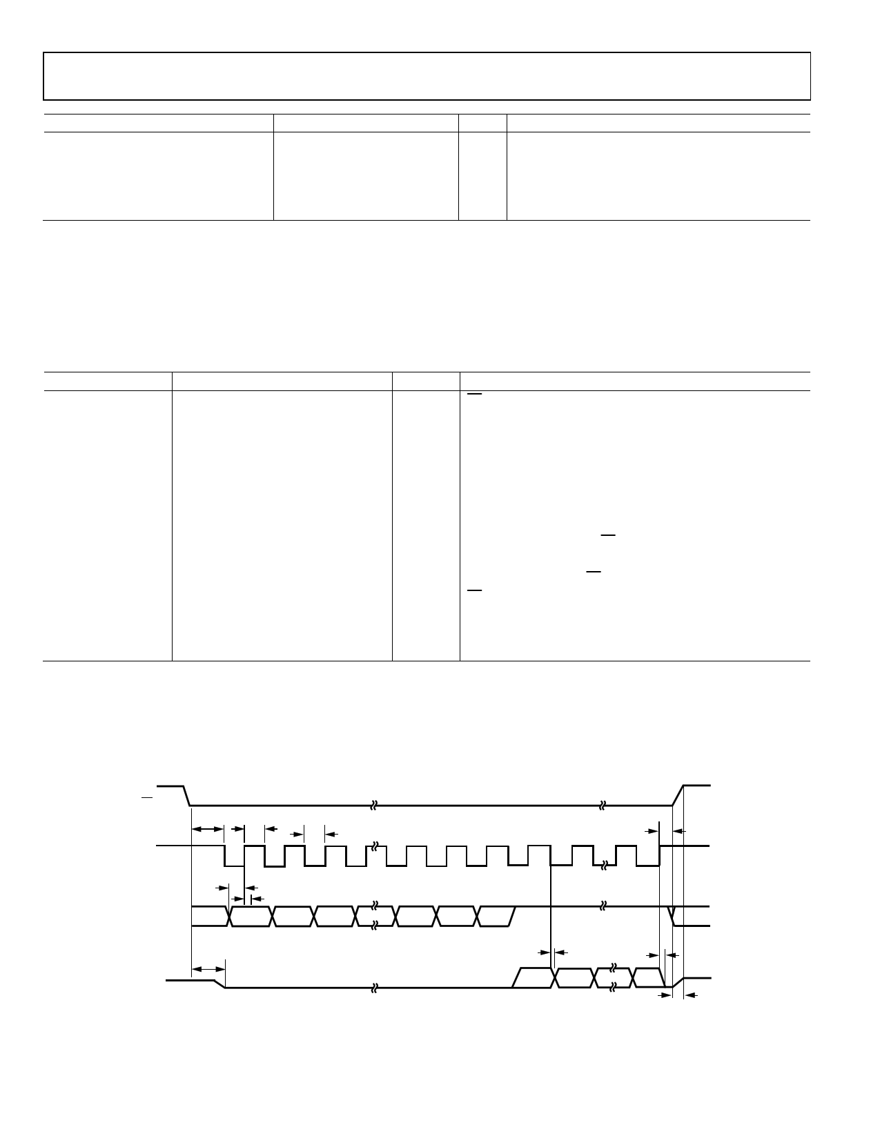
t1 t2
t3
12 3
t4
t5
MSB
678 9
LSB
t9
MSB
Figure 2. Detailed SPI Timing Diagram
10
t6
t8
23 24
t10
LSB
t7
Rev. 0 | Page 4 of 24
5 Page 
ADT7311
CS
Data Sheet
DIN
DOUT
0x08
0x20
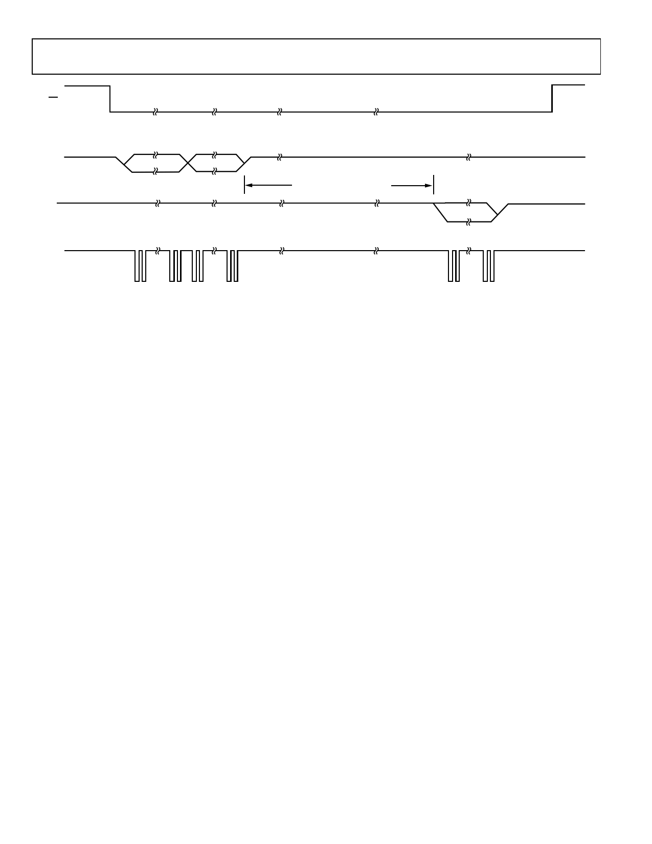
WAIT 240ms MINIMUM
FOR CONVERSION TO FINISH
DATA
SCLK
Figure 12. Typical SPI One-Shot Write to Configuration Register Followed by a Read from the Temperature Value Register
ONE-SHOT MODE
Setting Bit 6 to 0 and Bit 5 to 1 of the configuration register
(Register Address 0x01) enables the one-shot mode. When
this mode is enabled, the ADT7311 immediately completes a
conversion and then goes into shutdown mode.
Wait for a minimum of 240 ms after writing to the operation
mode bits before reading back the temperature from the
temperature value register. This time ensures that the ADT7311
has time to power up and complete a conversion.
To obtain an updated temperature conversion, reset the Bit 6 to
0 and Bit 5 to 1 in the configuration register (0x01).
The one-shot mode is useful when one of the circuit design
priorities is to reduce power consumption.
1 SPS MODE
In this mode, the part performs one measurement per second.
A conversion takes only 60 ms, and it remains in the idle state
for the remaining 940 ms period. This mode is enabled by
writing 1 to Bit 6 and 0 to Bit 5 of the configuration register
(Register Address 0x01).
Rev. 0 | Page 10 of 24
11 Page | ||
| Páginas | Total 25 Páginas | |
| PDF Descargar | [ Datasheet ADT7311.PDF ] | |
Hoja de datos destacado
| Número de pieza | Descripción | Fabricantes |
| ADT7310 | 16-Bit Digital SPI Temperature Sensor | Analog Devices |
| ADT7310 | system specific power supply IC | ADTech |
| ADT7311 | 16-Bit Digital SPI Temperature Sensor | Analog Devices |
| ADT7312 | Digital SPI Temperature Sensor | Analog Devices |
| Número de pieza | Descripción | Fabricantes |
| SLA6805M | High Voltage 3 phase Motor Driver IC. |
Sanken |
| SDC1742 | 12- and 14-Bit Hybrid Synchro / Resolver-to-Digital Converters. |
Analog Devices |
|
DataSheet.es es una pagina web que funciona como un repositorio de manuales o hoja de datos de muchos de los productos más populares, |
| DataSheet.es | 2020 | Privacy Policy | Contacto | Buscar |
