|
|
|
PDF AD5380 Data sheet ( Hoja de datos )
| Número de pieza | AD5380 | |
| Descripción | 14-Bit denseDAC | |
| Fabricantes | Analog Devices | |
| Logotipo | ||
Hay una vista previa y un enlace de descarga de AD5380 (archivo pdf) en la parte inferior de esta página. Total 30 Páginas | ||
|
No Preview Available !
Data Sheet
40-Channel, 3 V/5 V, Single-Supply,
14-Bit, denseDAC
AD5380
FEATURES
Guaranteed monotonic
INL error: ±4 LSB max
On-chip 1.25 V/2.5 V, 10 ppm/°C reference
Temperature range: –40°C to +85°C
Rail-to-rail output amplifier
Power down
Package type: 100-lead LQFP (14 mm × 14 mm)
User interfaces
Parallel
Serial (SPI®-, QSPI™-, MICROWIRE™-, DSP-compatible,
featuring data readback)
I2C®-compatible
Robust 6.5 kV HBM and 2 kV FICDM ESD rating
INTEGRATED FUNCTIONS
Channel monitor
Simultaneous output update via LDAC
Clear function to user programmable code
Amplifier boost mode to optimize slew rate
User programmable offset and gain adjust
Toggle mode enables square wave generation
Thermal monitor
APPLICATIONS
Variable optical attenuators (VOA)
Level setting (ATE)
Optical micro-electro-mechanical systems (MEMS)
Control systems
Instrumentation
DVDD (×3)
DGND (×3)
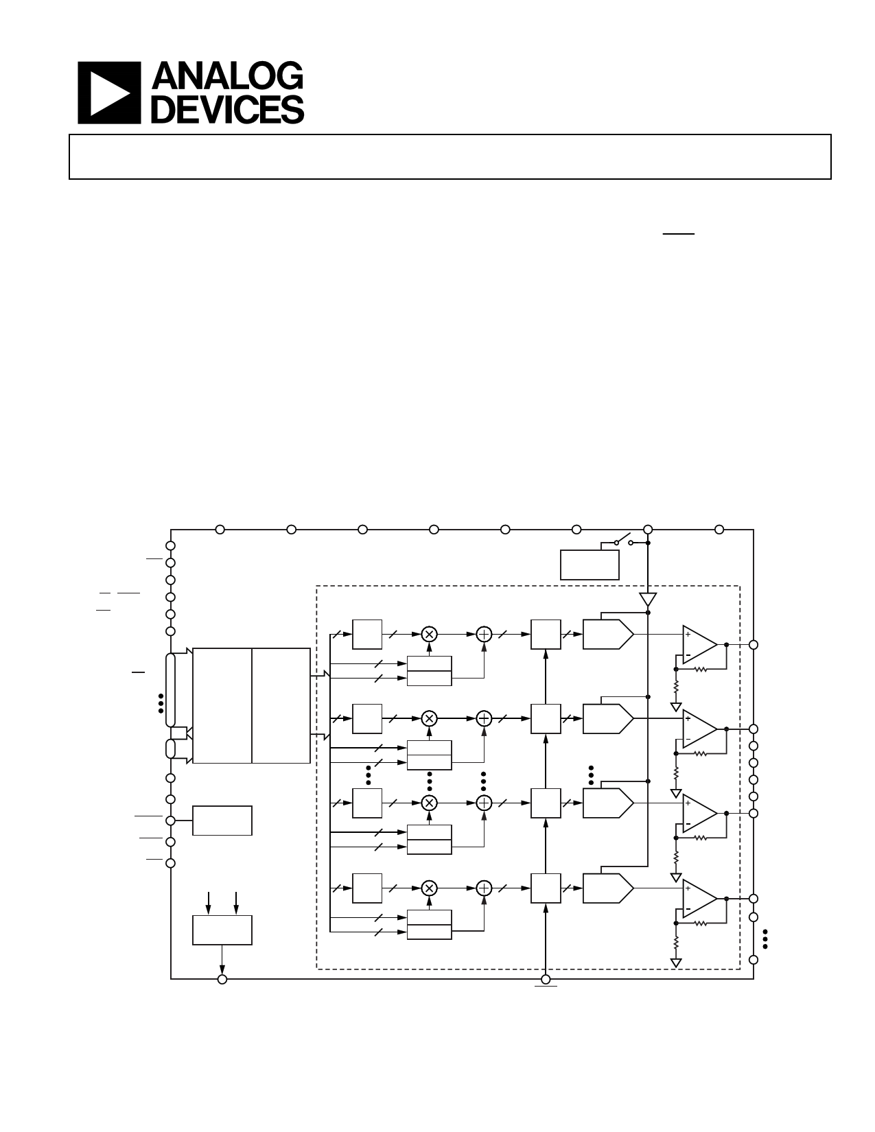
FUNCTIONAL BLOCK DIAGRAM
AVDD (×5)
AGND (×5) DAC_GND (×5)
REFGND REFOUT/REFIN SIGNAL_GND (×5)
PD
SER/PAR
FIFO EN
CS/(SYNC/AD0)
WR/(DCEN/AD1)
SDO
AD5380
DB13/(DIN/SDA)
DB12/(SCLK/SCL)
DB11/(SPI/I2C)
DB10
DB0
A5
A0
INTERFACE
CONTROL
LOGIC
FIFO
+
STATE
MACHINE
+
CONTROL
LOGIC
REG0
REG1
RESET
BUSY
CLR
POWER-ON
RESET
VOUT0………VOUT38
39-TO-1
MUX
14 INPUT 14
REG0
14
14
m REG0
c REG0
14 INPUT 14
REG1
14
14
m REG1
c REG1
14 INPUT 14
REG6
14
14
m REG6
c REG6
14 INPUT 14
REG7
14
14
m REG7
c REG7
×5
1.25V/2.5V
REFERENCE
14
DAC 14
REG0
DAC 0
14
DAC 14
REG1
DAC 1
14
DAC 14
REG6
DAC 6
14
DAC 14
REG7
DAC 7
R
R
R
R
R
R
R
R
VOUT
VOUT1
VOUT2
VOUT3
VOUT4
VOUT5
VOUT6
VOUT7
VOUT8
VOUT38
VOUT39/MON_OUT
Figure 1.
LDAC
Rev. D
Document Feedback
Information furnished by Analog Devices is believed to be accurate and reliable. However, no
responsibility is assumed by Analog Devices for its use, nor for any infringements of patents or other
rights of third parties that may result from its use. Specifications subject to change without notice. No
license is granted by implication or otherwise under any patent or patent rights of Analog Devices.
Trademarksandregisteredtrademarksarethepropertyoftheirrespectiveowners.
One Technology Way, P.O. Box 9106, Norwood, MA 02062-9106, U.S.A.
Tel: 781.329.4700 ©2004–2014 Analog Devices, Inc. All rights reserved.
Technical Support
www.analog.com
1 page 
AD5380
GENERAL DESCRIPTION
The AD5380 is a complete, single-supply, 40-channel, 14-bit
denseDAC® available in a 100-lead LQFP package. All 40
channels have an on-chip output amplifier with rail-to-rail
operation. The AD5380 includes a programmable internal
1.25 V/2.5 V, 10 ppm/°C reference, an on-chip channel monitor
function that multiplexes the analog outputs to a common
MON_OUT pin for external monitoring, and an output
amplifier boost mode that allows optimization of the amplifier
slew rate. The AD5380 contains a double-buffered parallel
interface that features a 20 ns WR pulse width, an SPI-, QSPI-,
-MICROWIRE, -DSP compatible serial interface with interface
speeds in excess of 30 MHz, and an I2C-compatible interface
that supports a 400 kHz data transfer rate.
Data Sheet
An input register followed by a DAC register provides double
buffering, allowing the DAC outputs to be updated
independently or simultaneously using the LDAC input.
Each channel has a programmable gain and offset adjust register
that allows the user to fully calibrate any DAC channel. Power
consumption is typically 0.25 mA/channel with boost off.
Rev. D | Page 4 of 40
5 Page 
AD5380
SCLK
SYNC
t4
t7
t3
t6
t8 t9
t1
24
t2 t5
24
DIN
BUSY
LDAC1
VOUT1
LDAC2
VOUT2
DB23
DB0
t10
t11
t12 t13
t15
t17
t14
t13
t16 t17
CLR
t18
t19
VOUT
1LDAC ACTIVE DURING BUSY.
2LDAC ACTIVE AFTER BUSY.
Figure 3. Serial Interface Timing Diagram (Standalone Mode)
SCLK
SYNC
DIN
SDO
SCLK
SYNC
DIN
SDO
LDAC
24
t7A
48
DB23
DB0
DB23
DB0
INPUT WORD SPECIFIES
REGISTER TO BE READ
DB23
NOP CONDITION
DB0
UNDEFINED
SELECTED REGISTER
DATA CLOCKED OUT
Figure 4. Serial Interface Timing Diagram (Data Readback Mode)
t7
t4
t1
24
t3 t2
48
t21
t22
t8 t9
DB23
DB0 DB23
DB0
INPUT WORD FOR DAC N
t20
INPUT WORD FOR DAC N+1
DB23
DB0
UNDEFINED
INPUT WORD FOR DAC N
t13
t23
Figure 5. Serial Interface Timing Diagram (Daisy-Chain Mode)
Rev. D | Page 10 of 40
Data Sheet
11 Page | ||
| Páginas | Total 30 Páginas | |
| PDF Descargar | [ Datasheet AD5380.PDF ] | |
Hoja de datos destacado
| Número de pieza | Descripción | Fabricantes |
| AD538 | Real-Time Analog Computational Unit ACU | Analog Devices |
| AD5380 | 14-Bit denseDAC | Analog Devices |
| AD5381 | Voltage Output DAC | Analog Devices |
| AD5382 | 14-Bit denseDAC | Analog Devices |
| Número de pieza | Descripción | Fabricantes |
| SLA6805M | High Voltage 3 phase Motor Driver IC. |
Sanken |
| SDC1742 | 12- and 14-Bit Hybrid Synchro / Resolver-to-Digital Converters. |
Analog Devices |
|
DataSheet.es es una pagina web que funciona como un repositorio de manuales o hoja de datos de muchos de los productos más populares, |
| DataSheet.es | 2020 | Privacy Policy | Contacto | Buscar |