|
|
|
PDF AD5313R Data sheet ( Hoja de datos )
| Número de pieza | AD5313R | |
| Descripción | Dual 10-Bit nanoDAC | |
| Fabricantes | Analog Devices | |
| Logotipo | ||
Hay una vista previa y un enlace de descarga de AD5313R (archivo pdf) en la parte inferior de esta página. Total 29 Páginas | ||
|
No Preview Available !
Data Sheet
Dual, 10-Bit nanoDAC
with 2 ppm/°C Reference, SPI Interface
AD5313R
FEATURES
Low drift 2.5 V reference: 2 ppm/°C typical
Tiny package: 3 mm × 3 mm, 16-lead LFCSP
Total unadjusted error (TUE): ±0.1% of FSR maximum
Offset error: ±1.5 mV maximum
Gain error: ±0.1% of FSR maximum
High drive capability: 20 mA, 0.5 V from supply rails
User selectable gain of 1 or 2 (GAIN pin)
Reset to zero scale or midscale (RSTSEL pin)
1.8 V logic compatibility
50 MHz SPI with readback or daisy chain
Low glitch: 0.5 nV-sec
Robust 4 kV HBM and 1.5 kV FICDM ESD ratings
Low power: 3.3 mW at 3 V
2.7 V to 5.5 V power supply
−40°C to +105°C temperature range
APPLICATIONS
Optical transceivers
Base station power amplifiers
Process control (PLC I/O cards)
Industrial automation
Data acquisition systems
GENERAL DESCRIPTION
The AD5313R, a member of the nanoDAC® family, is a low power,
dual, 10-bit buffered voltage output digital-to-analog converter
(DAC). The device includes a 2.5 V, 2 ppm/°C internal reference
(enabled by default) and a gain select pin giving a full-scale output
of 2.5 V (gain = 1) or 5 V (gain = 2). The AD5313R operates
from a single 2.7 V to 5.5 V supply, is guaranteed monotonic by
design, and exhibits less than 0.1% FSR gain error and 1.5 mV
offset error performance. The device is available in a 3 mm ×
3 mm LFCSP package and a TSSOP package.
The AD5313R also incorporates a power-on reset circuit and
a RSTSEL pin that ensures that the DAC outputs power up to
zero scale or midscale and remain there until a valid write occurs.
The part contains a per channel power-down feature that reduces
the current consumption of the device to 4 µA at 3 V while in
power-down mode.
The AD5313R employs a versatile serial peripheral interface
(SPI) that operates at clock rates up to 50 MHz, and the device
contains a VLOGIC pin that is intended for 1.8 V/3 V/5 V logic.
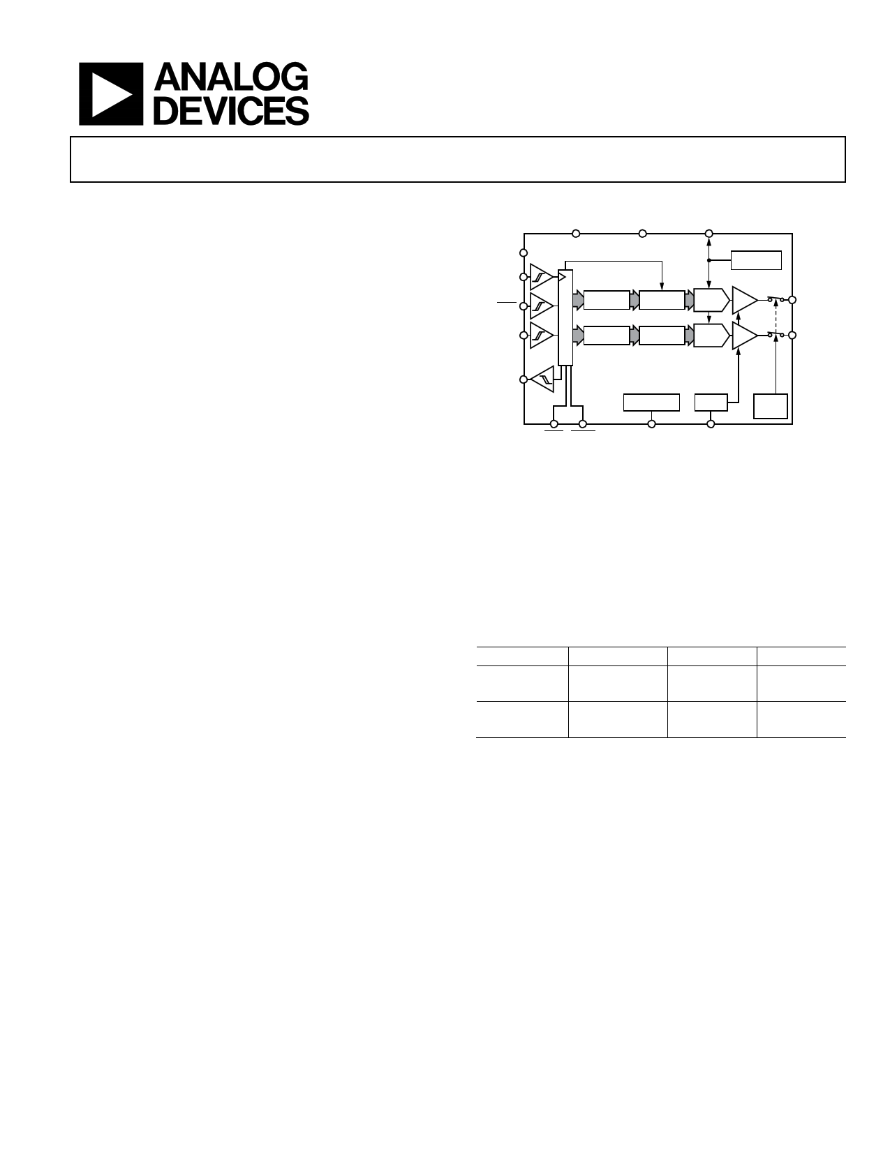
VLOGIC
SCLK
SYNC
SDIN
FUNCTIONAL BLOCK DIAGRAM
VDD
GND
VREF
AD5313R
2.5V
REFERENCE
INPUT
REGISTER
DAC
STRING
REGISTER DAC A
INPUT
REGISTER
DAC
STRING
REGISTER DAC B
BUFFER
BUFFER
VOUTA
VOUTB
SDO
LDAC RESET
POWER-ON
RESET
GAIN =
×1/×2
RSTSEL
Figure 1.
GAIN
POWER-
DOWN
LOGIC
Table 1. Related Devices
Interface
Reference
SPI Internal
External
I2C Internal
External
12-Bit
AD5687R
AD5687
AD5697R
N/A
10-Bit
N/A
AD53131
AD5338R1
AD53381
1 The AD5313R and the AD5313 are not pin-to-pin or software compatible;
likewise, the AD5338R and the AD5338 are not pin-to-pin or software
compatible.
PRODUCT HIGHLIGHTS
1. Precision DC Performance.
Total unadjusted error: ±0.1% of FSR maximum
Offset error: ±1.5 mV maximum
Gain error: ±0.1% of FSR maximum
2. Low Drift 2.5 V On-Chip Reference.
2 ppm/°C typical temperature coefficient
5 ppm/°C maximum temperature coefficient
3. Two Package Options.
3 mm × 3 mm, 16-lead LFCSP
16-lead TSSOP
Rev. A
Document Feedback
Information furnished by Analog Devices is believed to be accurate and reliable. However, no
responsibility is assumed by Analog Devices for its use, nor for any infringements of patents or other
rights of third parties that may result from its use. Specifications subject to change without notice. No
license is granted by implication or otherwise under any patent or patent rights of Analog Devices.
Trademarksandregisteredtrademarksarethepropertyoftheirrespectiveowners.
One Technology Way, P.O. Box 9106, Norwood, MA 02062-9106, U.S.A.
Tel: 781.329.4700
©2014 Analog Devices, Inc. All rights reserved.
Technical Support
www.analog.com
1 page 
AD5313R
Data Sheet
Parameter
LOGIC OUTPUTS (SDO)2
Output Low Voltage (VOL)
Output High Voltage (VOH)
Floating State Output Capacitance
POWER REQUIREMENTS
VLOGIC
ILOGIC
VDD
IDD
Normal Mode9
All Power-Down Modes10
Min Typ
VLOGIC − 0.4
4
1.8
2.7
VREF + 1.5
0.59
1.1
1
Max
0.4
5.5
3
5.5
5.5
0.7
1.3
4
6
Unit
V
V
pF
V
µA
V
V
mA
mA
µA
µA
Test Conditions/Comments
ISINK = 200 µA
ISOURCE = 200 µA
Gain = 1
Gain = 2
VIH = VDD, VIL = GND, VDD = 2.7 V to 5.5 V
Internal reference off
Internal reference on, at full scale
−40°C to +85°C
−40°C to +105°C
1 DC specifications tested with the outputs unloaded, unless otherwise noted. Upper dead band = 10 mV; it exists only when VREF = VDD with gain = 1 or when VREF/2 =
VDD with gain = 2. Linearity calculated using a reduced code range of 4 to 1020.
2 Guaranteed by design and characterization; not production tested.
3 Channel A can have an output current of up to 30 mA. Similarly, Channel B can have an output current of up to 30 mA, up to a junction temperature of 110°C.
4 VDD = 5 V. The device includes current limiting that is intended to protect the device during temporary overload conditions. Junction temperature may be exceeded
during current limit, but operation above the specified maximum operation junction temperature can impair device reliability.
5 When drawing a load current at either rail, the output voltage headroom with respect to that rail is limited by the 25 Ω typical channel resistance of the output
devices. For example, when sinking 1 mA, the minimum output voltage = 25 Ω × 1 mA = 25 mV (see Figure 28).
6 Initial accuracy presolder reflow is ±750 µV; output voltage includes the effects of preconditioning drift. See the Internal Reference Setup section.
7 Reference is trimmed and tested at two temperatures and is characterized from −40°C to +105°C.
8 Reference temperature coefficient is calculated as per the box method. See the Terminology section for more information.
9 Interface is inactive, both DACs are active, and DAC outputs are unloaded.
10 Both DACs are powered down.
AC CHARACTERISTICS
VDD = 2.7 V to 5.5 V; RL = 2 kΩ to GND; CL = 200 pF to GND; 1.8 V ≤ VLOGIC ≤ 5.5 V; all specifications TMIN to TMAX, unless otherwise noted.
Temperature range = −40°C to +105°C, typical at 25°C. Guaranteed by design and characterization; not production tested.
Table 3.
Parameter1
Output Voltage Settling Time
Slew Rate
Digital-to-Analog Glitch Impulse
Digital Feedthrough
Digital Crosstalk
Analog Crosstalk
DAC-to-DAC Crosstalk
Total Harmonic Distortion (THD)2
Output Noise Spectral Density (NSD)
Output Noise
Signal-to-Noise Ratio (SNR)
Spurious Free Dynamic Range (SFDR)
Signal-to-Noise-and-Distortion Ratio
(SINAD)
Min
Typ Max
57
0.8
0.5
0.13
0.1
0.2
0.3
−80
300
6
90
83
80
Unit
µs
V/µs
nV-sec
nV-sec
nV-sec
nV-sec
nV-sec
dB
nV/√Hz
µV p-p
dB
dB
dB
Test Conditions/Comments
¼ to ¾ scale settling to ±2 LSB
1 LSB change around major carry
At ambient, BW = 20 kHz, VDD = 5 V, fOUT = 1 kHz
DAC code = midscale, 10 kHz; gain = 2
0.1 Hz to 10 Hz
At ambient, BW = 20 kHz, VDD = 5 V, fOUT = 1 kHz
At ambient, BW = 20 kHz, VDD = 5 V, fOUT = 1 kHz
At ambient, BW = 20 kHz, VDD = 5 V, fOUT = 1 kHz
1 See the Terminology section.
2 Digitally generated sine wave at 1 kHz.
Rev. A | Page 4 of 28
5 Page 
AD5313R
TYPICAL PERFORMANCE CHARACTERISTICS
2.5020
2.5015
2.5010
DEVICE 1
DEVICE 2
DEVICE 3
DEVICE 4
DEVICE 5
VDD = 5V
2.5005
2.5000
2.4995
2.4990
2.4985
2.4980
–40 –20 0 20 40 60 80 100 120
TEMPERATURE (°C)
Figure 8. Internal Reference Voltage vs. Temperature
90
VDD = 5V
80
70
60
50
40
30
20
10
0
0 0.5 1.0 1.5 2.0 2.5 3.0 3.5 4.0 4.5 5.0
TEMPERATURE DRIFT (ppm/°C)
Figure 9. Reference Output Temperature Drift Histogram
1600 VDD = 5V
TA = 25°C
1400
1200
1000
800
600
400
200
0
10 100 1k 10k 100k 1M
FREQUENCY (MHz)
Figure 10. Internal Reference Noise Spectral Density vs. Frequency
VDD = 5V
TA = 25°C
1
Data Sheet
T
CH1 10µV
M1.0s
A CH1 160mV
Figure 11. Internal Reference Noise, 0.1 Hz to 10 Hz
2.5000
2.4999
VDD = 5V
TA = 25°C
2.4998
2.4997
2.4996
2.4995
2.4994
2.4993
–0.005
–0.003
–0.001
0.001
ILOAD (A)
0.003
0.005
Figure 12. Internal Reference Voltage vs. Load Current
2.5002
2.5000
TA = 25°C
D1
2.4998
2.4996
D3
2.4994
2.4992
D2
2.4990
2.5 3.0 3.5 4.0 4.5 5.0 5.5
VDD (V)
Figure 13. Internal Reference Voltage vs. Supply Voltage
Rev. A | Page 10 of 28
11 Page | ||
| Páginas | Total 29 Páginas | |
| PDF Descargar | [ Datasheet AD5313R.PDF ] | |
Hoja de datos destacado
| Número de pieza | Descripción | Fabricantes |
| AD5313 | +2.5 V to +5.5 V/ 230 uA/ Dual Rail-to-Rail Voltage Output 8-/10-/12-Bit DACs | Analog Devices |
| AD5313R | Dual 10-Bit nanoDAC | Analog Devices |
| Número de pieza | Descripción | Fabricantes |
| SLA6805M | High Voltage 3 phase Motor Driver IC. |
Sanken |
| SDC1742 | 12- and 14-Bit Hybrid Synchro / Resolver-to-Digital Converters. |
Analog Devices |
|
DataSheet.es es una pagina web que funciona como un repositorio de manuales o hoja de datos de muchos de los productos más populares, |
| DataSheet.es | 2020 | Privacy Policy | Contacto | Buscar |