|
|
|
PDF ADA4856-3 Data sheet ( Hoja de datos )
| Número de pieza | ADA4856-3 | |
| Descripción | Rail-to-Rail Output Video Amplifier | |
| Fabricantes | Analog Devices | |
| Logotipo | ||
Hay una vista previa y un enlace de descarga de ADA4856-3 (archivo pdf) en la parte inferior de esta página. Total 21 Páginas | ||
|
No Preview Available !
Data Sheet
Single-Supply, High Speed, Fixed G = +2,
Rail-to-Rail Output Video Amplifier
ADA4856-3
FEATURES
Voltage feedback architecture
Rail-to-rail output swing: 0.1 V to 4.9 V
High speed amplifier
−3 dB bandwidth: 225 MHz
0.1 dB flatness at 2 V p-p: 74 MHz
Slew rate: 800 V/μs
Settling time to 0.1% with 2 V step: 5 ns
High input common-mode voltage range
−VS − 0.2 V to +VS − 1 V
Supply range: 3 V to 5.5 V
Differential gain error: 0.01%
Differential phase error: 0.01°
Low power
7.8 mA/amplifier typical supply current
Power-down feature
Available in 16-lead LFCSP
APPLICATIONS
Professional video
Consumer video
Imaging
Instrumentation
Base stations
Active filters
Buffers
GENERAL DESCRIPTION
The ADA4856-3 (triple) is a fixed gain of +2, single-supply, rail-
to-rail output video amplifier. It provides excellent video
performance with 225 MHz, −3 dB bandwidth, 800 V/μs slew rate,
and 74 MHz, 0.1 dB flatness into a 150 Ω load. It has a wide
input common-mode voltage range that extends 0.2 V below
ground and 1 V below the positive rail. In addition, the output
voltage swings within 200 mV of either supply, making this video
amplifier easy to use on single-supply voltages as low as 3.3 V.
The ADA4856-3 offers a typical low power of 7.8 mA per amplifier,
while being capable of delivering up to 52 mA of load current.
It also features a power-down function for power sensitive
applications that reduces the supply current to 1 mA.
The ADA4856-3 is available in a 16-lead LFCSP and is designed
to work over the extended industrial temperature range of
−40°C to +105°C.
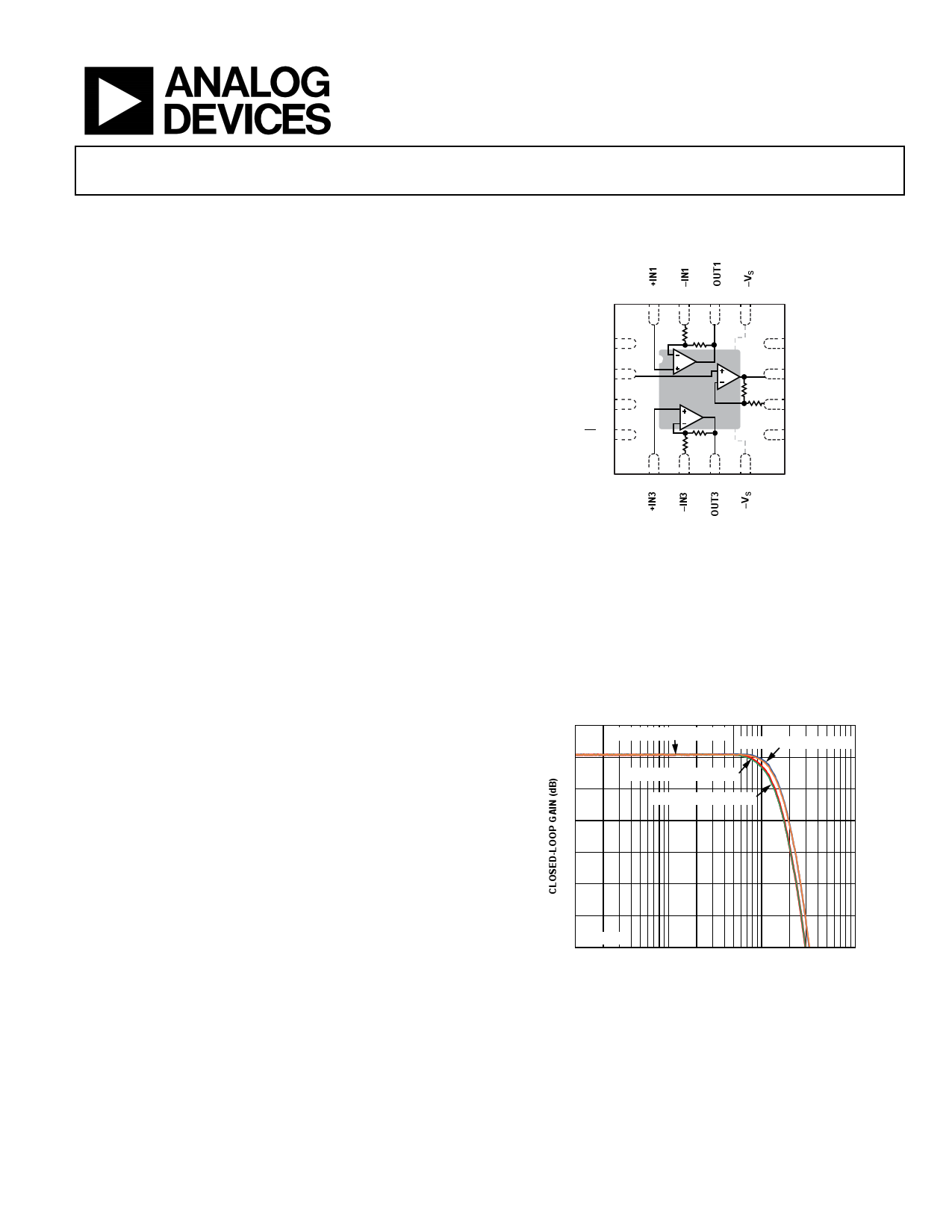
CONNECTION DIAGRAM
16 15 14 13
NC 1
+IN2 2
NC 3
PD 4
ADA4856-3
12 +VS
11 OUT2
10 –IN2
9 +VS
5 6 78
NOTES
1. NC = NO CONNECT.
2. EXPOSED PAD CONNECTED TO –VS.
Figure 1.
7 VS = 5V, VOUT = 1.4V p-p VS = 3.3V, VOUT = 1.4V p-p
6
VS = 3.3V, VOUT = 2V p-p
5
VS = 5V, VOUT = 2V p-p
4
3
2
1
RL = 150Ω
0
1
10 100
FREQUENCY (MHz)
Figure 2. Large Signal Frequency Response
1000
Rev. B
Document Feedback
Information furnished by Analog Devices is believed to be accurate and reliable. However, no
responsibility is assumed by Analog Devices for its use, nor for any infringements of patents or other
rights of third parties that may result from its use. Specifications subject to change without notice. No
license is granted by implication or otherwise under any patent or patent rights of Analog Devices.
Trademarksandregisteredtrademarksarethepropertyoftheirrespectiveowners.
One Technology Way, P.O. Box 9106, Norwood, MA 02062-9106, U.S.A.
Tel: 781.329.4700 ©2008–2013 Analog Devices, Inc. All rights reserved.
Technical Support
www.analog.com
1 page 
ADA4856-3
Data Sheet
3.3 V OPERATION
TA = 25°C, +VS = 3.3 V, −VS = 0 V, G = +2, RL = 150 Ω to midsupply, unless otherwise noted.
Table 2.
Parameter
DYNAMIC PERFORMANCE
−3 dB Bandwidth
Bandwidth for 0.1 dB Flatness
Slew Rate
Settling Time to 0.1% (Rise/Fall)
NOISE/DISTORTION PERFORMANCE
Harmonic Distortion (HD2/HD3)
Crosstalk, Output to Output
Input Voltage Noise
Input Current Noise
Differential Gain Error
Differential Phase Error
DC PERFORMANCE
Input Offset Voltage
Input Offset Voltage Drift
Input Bias Current
Input Offset Current
Closed-Loop Gain
Open-Loop Gain
INPUT CHARACTERISTICS
Input Resistance
Input Capacitance
Input Common-Mode Voltage Range
Common-Mode Rejection Ratio
OUTPUT CHARACTERISTICS
Output Voltage Swing
Linear Output Current Per Amplifier
POWER-DOWN
Turn-On Time
Turn-Off Time
Turn-On Voltage
POWER SUPPLY
Operating Range
Quiescent Current per Amplifier
Quiescent Current When Powered Down
Power Supply Rejection Ratio
Test Conditions
VO = 0.1 V p-p
VO = 2 V p-p
VO = 2 V p-p
VO = 2 V step
VO = 2 V step
fC = 5 MHz, VO = 1 V p-p, RL = 1 kΩ
fC = 20 MHz, VO = 1 V p-p, RL = 1 kΩ
f = 5 MHz
f = 100 kHz
f = 100 kHz
VCM = −0.2 V to +2.3 V
HD2 ≤ −60 dBc, RL = 10 Ω
∆VS = 2.97 V to 3.63 V
Min
1.95
−VS − 0.2
3
Typ
370
225
77
800
4.8/7
−95/−128
−74/−101
−78
14
2
0.01
0.01
1.2
5.5
−3.8
±0.05
2
90
3.2
0.5
94
0.1 to 3.22
49
78
950
2.05
7.5
0.98
94
Max
3
2.05
+VS − 1
5.5
Unit
MHz
MHz
MHz
V/µs
ns
dBc
dBc
dB
nV/√Hz
pA/√Hz
%
Degrees
mV
µV/°C
µA
µA
V/V
dB
MΩ
pF
V
dB
V
mA
ns
ns
V
V
mA
mA
dB
Rev. B | Page 4 of 20
5 Page 
ADA4856-3
0.08
0.06
0.04
0.02
0
CL = 2.2pF
CL = 4.4pF
CL = 6.6pF
–0.02
–0.04
–0.06
–0.08
VS = 3.3V
TIME (10ns/DIV)
Figure 23. Small Signal Transient Response vs. Capacitive Load
4
2 × VIN
3
2
VOUT
1
0
–1
–2
–3
–4
TIME (50ns/DIV)
Figure 24. Output Overdrive Recovery
3.0
VPD
2.5
2.0
1.5
VOUT
1.0
0.5
0
–0.5
–1.0
–1.5
TIME (1us/DIV)
Figure 25. Turn-On/Turn-Off Time
Data Sheet
1.5
1.0
0.5 CL = 2.2pF
CL = 4.4pF
CL = 6.6pF
0
–0.5
–1.0
–1.5
VS = 3.3V
TIME (10ns/DIV)
Figure 26. Large Signal Transient Response vs. Capacitive Load
2.5
2.0 2 × VIN
1.5
1.0 VOUT
0.5
0
–0.5
–1.0
–1.5
–2.0 VS = 3.3V
–2.5
TIME (50ns/DIV)
Figure 27. Output Overdrive Recovery
23.6
VS = 5V
23.4
23.2
23.0
22.8
22.6
22.4 VS = 3.3V
22.2
22.0
21.8
–40 –25 –10 5 20 35 50 65 80 95 110 125
TEMPERATURE (°C)
Figure 28. Quiescent Current vs. Temperature
Rev. B | Page 10 of 20
11 Page | ||
| Páginas | Total 21 Páginas | |
| PDF Descargar | [ Datasheet ADA4856-3.PDF ] | |
Hoja de datos destacado
| Número de pieza | Descripción | Fabricantes |
| ADA4856-3 | Rail-to-Rail Output Video Amplifier | Analog Devices |
| Número de pieza | Descripción | Fabricantes |
| SLA6805M | High Voltage 3 phase Motor Driver IC. |
Sanken |
| SDC1742 | 12- and 14-Bit Hybrid Synchro / Resolver-to-Digital Converters. |
Analog Devices |
|
DataSheet.es es una pagina web que funciona como un repositorio de manuales o hoja de datos de muchos de los productos más populares, |
| DataSheet.es | 2020 | Privacy Policy | Contacto | Buscar |