|
|
PDF ADA4303-2 Data sheet ( Hoja de datos )
| Número de pieza | ADA4303-2 | |
| Descripción | Low Cost Active RF Splitter | |
| Fabricantes | Analog Devices | |
| Logotipo |  |
|
Hay una vista previa y un enlace de descarga de ADA4303-2 (archivo pdf) en la parte inferior de esta página. Total 13 Páginas | ||
|
No Preview Available !
Data Sheet
FEATURES
Ideal for CATV applications
Excellent frequency response
1.7 GHz, −3 dB bandwidth
1 dB flatness to 1.2 GHz
Low noise figure: 4.4 dB
Low distortion
Composite second order (CSO): −62 dBc
Composite triple beat (CTB): −72 dBc
1 dB compression point of 8.5 dBm
3 dB of gain per output channel
24 dB isolation between output channels
75 Ω input and outputs
Small package size
12-lead, 3 mm × 3 mm lead frame chip scale package
APPLICATIONS
Set-top boxes
Home gateways
CATV distribution systems
Splitter modules
Digital cable ready (DCR) TVs
GENERAL DESCRIPTION
The ADA4303-2 is a 75 Ω, two-output active splitter for use
in applications where a lossless signal split is required. Typical
applications include multituner digital set-top boxes, cable splitter
modules, multituner/digital cable ready (DCR) televisions, and
home gateways where traditional solutions require discrete
passive splitter modules with separate fixed gain amplifiers.
The ADA4303-2 is a low cost alternative that simplifies designs
and improves system performance by integrating a signal splitter
element and a gain block into a single IC. The ADA4303-2 is
available in a 12-lead chip scale package (LFCSP) and operates
in the extended industrial temperature range of −40°C to +85°C.
1:2 Single-Ended, Low Cost
Active RF Splitter
ADA4303-2
FUNCTIONAL BLOCK DIAGRAM
5V 5V
0.1µF
0.1µF
1µH
VCC
IL
0.01µF
VIN
VO1
ADA4303-2
0.01µF
VO2
0.01µF
GND
249Ω
249Ω
Figure 1.
4
3
2
1
0
–1
–2
–3
–4
–5
–6
–7
–8
50
TA = –40°C
TA = +25°C
TA = +85°C
100 1000
FREQUENCY (MHz)
Figure 2. Gain (S21) vs. Frequency
4000
Rev. A
Document Feedback
Information furnished by Analog Devices is believed to be accurate and reliable. However, no
responsibilityisassumedbyAnalogDevices for itsuse,nor foranyinfringementsofpatentsor other
rights of third parties that may result from its use. Specifications subject to change without notice. No
license is granted by implication or otherwise under any patent or patent rights of Analog Devices.
Trademarksandregisteredtrademarksarethepropertyoftheirrespectiveowners.
One Technology Way, P.O. Box 9106, Norwood, MA 02062-9106, U.S.A.
Tel: 781.329.4700 ©2006–2016 Analog Devices, Inc. All rights reserved.
Technical Support
www.analog.com
1 page 
ADA4303-2
ABSOLUTE MAXIMUM RATINGS
Table 2.
Parameter
Supply Voltage
Power Dissipation
Storage Temperature Range
Operating Temperature Range
Lead Temperature (Soldering, 10 sec)
Junction Temperature
Rating
5.5 V
See Figure 3
−65°C to +125°C
−40°C to +85°C
300°C
150°C
Stresses at or above those listed under Absolute Maximum
Ratings may cause permanent damage to the product. This
is a stress rating only; functional operation of the product
at these or any other conditions above those indicated in
the operational section of this specification is not implied.
Operation beyond the maximum operating conditions for
extended periods may affect product reliability.
THERMAL RESISTANCE
θJA is specified for the worst-case conditions; that is, θJA is
specified for a device (including exposed pad) soldered to
the circuit board.
Table 3. Thermal Resistance
Package Type
12-Lead LFCSP (exposed pad)
θJA Unit
99.2 °C/W
Maximum Power Dissipation
The maximum safe power dissipation in the ADA4303-2
package is limited by the associated rise in junction temp-
erature (TJ) on the die. At approximately 150°C, which is the
glass transition temperature, the plastic changes the properties.
Even temporarily exceeding this temperature limit can change
the stresses that the package exerts on the die, permanently
shifting the parametric performance of the ADA4303-2.
Exceeding a junction temperature of 150°C for an extended
period can result in changes in the silicon devices,
potentially causing failure.
Data Sheet
The power dissipated in the package (PD) is the sum of the
quiescent power dissipation and the power dissipated in the
package due to the load drive. The quiescent power is the
voltage between the supply pins (VS) times the quiescent
current (IS). The power dissipated due to the load drive depends
upon the particular application. The power due to load drive is
calculated by multiplying the load current by the associated
voltage drop across the device. RMS voltages and currents must
be used in these calculations.
Airflow increases heat dissipation, effectively reducing θJA. In
addition, more metal directly in contact with the package
leads/exposed pad from metal traces, through-holes, ground,
and power planes reduces the θJA.
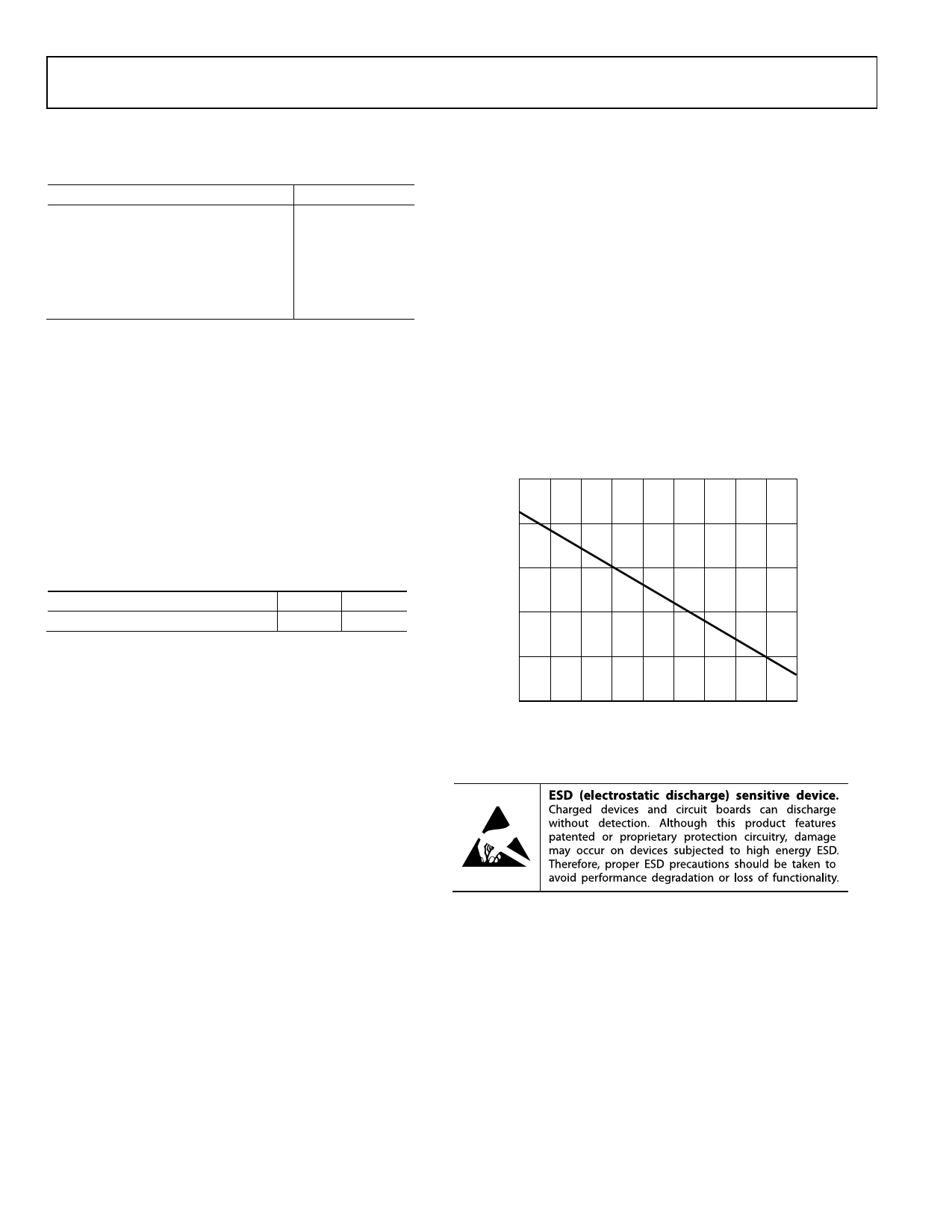
Figure 3 shows the maximum safe power dissipation in the
package vs. the ambient temperature for the 12-lead LFCSP
(99.2°C/W) on a JEDEC standard 4-layer board.
2.5
2.0
1.5
1.0
0.5
0
–60 –40 –20
0
20 40 60 80
AMBIENT TEMPERATURE (°C)
100 120
Figure 3. Maximum Power Dissipation vs. Temperature for a 4-Layer Board
ESD CAUTION
Rev. A | Page 4 of 12
5 Page 
ADA4303-2
NOTES
Data Sheet
Rev. A | Page 10 of 12
11 Page | ||
| Páginas | Total 13 Páginas | |
| PDF Descargar | [ Datasheet ADA4303-2.PDF ] | |
Hoja de datos destacado
| Número de pieza | Descripción | Fabricantes |
| ADA4303-2 | Low Cost Active RF Splitter | Analog Devices |
| ADA4303-2 | Low Cost Active RF Splitter | Analog Devices |
| Número de pieza | Descripción | Fabricantes |
| SLA6805M | High Voltage 3 phase Motor Driver IC. |
Sanken |
| SDC1742 | 12- and 14-Bit Hybrid Synchro / Resolver-to-Digital Converters. |
Analog Devices |
|
DataSheet.es es una pagina web que funciona como un repositorio de manuales o hoja de datos de muchos de los productos más populares, |
| DataSheet.es | 2020 | Privacy Policy | Contacto | Buscar |
