|
|
|
PDF ADA4312-1 Data sheet ( Hoja de datos )
| Número de pieza | ADA4312-1 | |
| Descripción | High Output Current Line Driver | |
| Fabricantes | Analog Devices | |
| Logotipo | ||
Hay una vista previa y un enlace de descarga de ADA4312-1 (archivo pdf) en la parte inferior de esta página. Total 13 Páginas | ||
|
No Preview Available !
Data Sheet
Wideband, Differential, High Output Current
Line Driver with Shutdown
ADA4312-1
FEATURES
High speed
−3 dB bandwidth: 195 MHz, GDIFF = +16 V/V, RL, DIFF = 40 Ω
Differential slew rate: 2100 V/µs
Wide output swing: 18.0 V p-p differential, 12 V supply
High output current: 225 mA peak
G.hn MTPR at 16 dBm line power
−64 dBc typical at 5 MHz, referred to −58 dBm/Hz
−64 dBc typical at 17 MHz, referred to −58 dBm/Hz
−64 dBc typical at 28 MHz, referred to −58 dBm/Hz
−63 dBc typical at 31 MHz, referred to −58 dBm/Hz
−61 dBc typical at 59 MHz, referred to −58 dBm/Hz
−62 dBc typical at 82 MHz, referred to −58 dBm/Hz
Shutdown
CMOS-compatible SD pin
Shutdown quiescent current: 3 mA
ZOUT in shutdown: 10 kΩ differential (open-loop)
Resistor adjustable quiescent current
APPLICATIONS
ITU G.hn (ITU G.9960/G.9961)
HomePlug AV
HomePlug AV2
IEEE 1901
GENERAL DESCRIPTION
The ADA4312-1 is a high speed, differential, current feedback line
driver designed for half-duplex G.hn power line communication
(PLC) modems. The high output current, high bandwidth, and
slew rate of 2100 V/µs make the ADA4312-1 an excellent choice
for G.hn broadband applications that require high linearity
while driving low impedance loads.
The CMOS-compatible shutdown control pin (SD) reduces
the quiescent current to 3 mA while maintaining an output
impedance of 10 kΩ differential. The ADA4312-1 also provides
resistor adjustable quiescent current for improved efficiency in
transmit mode.
The ADA4312-1 is available in a thermally enhanced, 16-lead
LFCSP with an exposed pad to facilitate robust thermal
management. The ADA4312-1 is rated to operate over the
extended industrial temperature range of −40°C to +85°C.
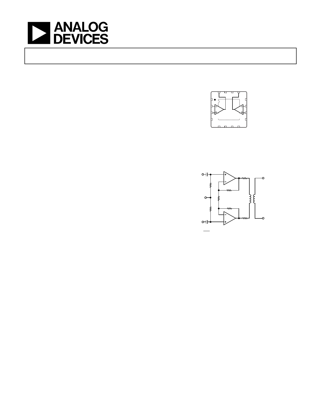
FUNCTIONAL BLOCK DIAGRAM
NC 1
–IN A 2
+IN A 3
GND 4
ADA4312-1
12 NC
11 –IN B
10 +IN B
9 SD
NC = NO CONNECT. DO NOT CONNECT
TO THIS PIN.
Figure 1. Thermally Enhanced, 4 mm × 4 mm, 16-Lead LFCSP_WQ
TYPICAL APPLICATION CIRCUIT
VMID*
1/2
ADA4312-1
1/2
VMID
=
VCC
2
ADA4312-1
Figure 2. Typical PLC Driver Application
Rev. 0
Document Feedback
Information furnished by Analog Devices is believed to be accurate and reliable. However, no
responsibilityisassumedbyAnalogDevices for itsuse,nor foranyinfringementsofpatentsor other
rights of third parties that may result from its use. Specifications subject to change without notice. No
license is granted by implication or otherwise under any patent or patent rights of Analog Devices.
Trademarksandregisteredtrademarksarethepropertyoftheirrespectiveowners.
One Technology Way, P.O. Box 9106, Norwood, MA 02062-9106, U.S.A.
Tel: 781.329.4700
©2012 Analog Devices, Inc. All rights reserved.
Technical Support
www.analog.com
1 page 
ADA4312-1
ABSOLUTE MAXIMUM RATINGS
Table 2.
Parameter
Supply Voltage, VCC
SD Voltage
Power Dissipation
Storage Temperature Range
Operating Temperature Range
Lead Temperature (Soldering, 10 sec)
Junction Temperature
Rating
13.2 V
VCC
1.25 W
−65°C to +125°C
−40°C to +85°C
300°C
150°C
Stresses above those listed under Absolute Maximum Ratings
may cause permanent damage to the device. This is a stress
rating only; functional operation of the device at these or any
other conditions above those indicated in the operational
section of this specification is not implied. Exposure to absolute
maximum rating conditions for extended periods may affect
device reliability.
THERMAL RESISTANCE
The thermal resistance (θJA) was specified using the ADA4312-1
evaluation board (EVAL-ADA4312-1ACPZ).
Table 3.
Package Type
16-Lead LFCSP_WQ
θJA
31.8
Unit
°C/W
Data Sheet
MAXIMUM POWER DISSIPATION
Exceeding a junction temperature of 150°C can result in changes
to silicon devices, potentially causing degradation or loss of
functionality.
The power dissipation of the ADA4312-1 is 750 mW for a typical
G.hn application delivering 16 dBm into a 40 Ω differential load.
The maximum internal power dissipation should not exceed
1.25 W over the extended industrial temperature range of −40°C
to +85°C on a PCB designed according to the guidelines in the
Thermal Management section.
ESD CAUTION
Rev. 0 | Page 4 of 12
5 Page 
ADA4312-1
Note that there is a trade-off between the adjusted quiescent
current and the linearity (or MTPR) of the transmitted signal.
Multitone power ratio (MTPR) was monitored at 5 MHz,
17 MHz, 28 MHz, 31 MHz, 59 MHz, and 82 MHz. Figure 18
can be used to gauge the approximate degradation of MTPR
vs. RIADJ and quiescent current while transmitting the G.hn
signal across a 40 Ω differential load in the circuit shown in
Figure 17.
–40
–45
–50 8kΩ, IQ = 11mA
–55 4kΩ, IQ = 18mA
–60 2kΩ, IQ = 26mA
–65 0Ω, IQ = 46.5mA
1kΩ, IQ = 33mA
–70
0
10 20 30 40 50 60 70 80 90
FREQUENCY (MHz)
Figure 18. MTPR vs. RIADJ
PCB LAYOUT
As is the case with many high speed line driver applications, care-
ful attention to printed circuit board (PCB) layout can improve
performance and help maintain stability while preventing excessive
die temperatures during normal operation. Differential signal
balance can be maintained by using symmetry in the PCB layout
of input and output signal traces.
Keeping the input and output traces as short as possible helps
prevent excessive parasitics from affecting overall performance
and stability. Keep the feedback resistors and gain setting resistor
as close to the line driver as physically possible. The back termi-
nation resistors and line coupling transformer should be placed
as close to the ADA4312-1 outputs as possible.
For more information about high speed board layout, see A
Practical Guide to High-Speed Printed-Circuit-Board Layout
(Analog Dialogue, Volume 39, September 2005).
Data Sheet
THERMAL MANAGEMENT
The thermal pad of the ADA4312-1 is an electrically isolated
copper pad that should be soldered to an external thermal
ground plane. The number of thermal vias that connect the
exposed pad of the ADA4312-1 to the PCB can influence the
thermal conductivity of the PCB assembly. Moving heat away
from the ADA4312-1 die to the ambient environment is the
objective of a PCB designed in accordance with the guidelines
found in the AN-772 Application Note.
The outer layers of the PCB are the best choice to radiate heat
into the environment by convection. Conducting heat away
from the ADA4312-1 die into the outer layers of the PCB can
be accomplished with nine thermal vias connecting the exposed
pad to both outer layers. The vias can be spaced 0.75 mm apart
in a 3 × 3 matrix.
The ADA4312-1 evaluation board (EVAL-ADA4312-1ACPZ)
represents a robust example of an effective thermal management
approach (see Figure 19 and Figure 20).
For more information about thermal management, solder
assembly techniques for LFCSP packages, and important
package mechanical and materials information, refer to the
following link:
http://www.analog.com/en/technical-library/packages/csp-
chip-scale-package/lfcsp/index.html
POWER SUPPLY BYPASSING
The ADA4312-1 should be operated on a well-regulated single
+12 V power supply. Pay careful attention to power supply
decoupling. Use high quality capacitors with low equivalent series
resistance (ESR), such as multilayer ceramic capacitors (MLCCs),
to minimize supply voltage ripple and power dissipation.
Locate the 0.1 µF MLCC decoupling capacitor no more than
one-eighth of an inch away from the VCC supply pin. In addition,
a 10 µF tantalum capacitor is recommended to provide good
decoupling for lower frequency signals and to supply current for
fast, large signal changes at the ADA4312-1 outputs. Lay out
bypassing capacitors to keep return currents away from the
inputs of the amplifiers. A large ground plane provides a low
impedance path for the return currents.
Rev. 0 | Page 10 of 12
11 Page | ||
| Páginas | Total 13 Páginas | |
| PDF Descargar | [ Datasheet ADA4312-1.PDF ] | |
Hoja de datos destacado
| Número de pieza | Descripción | Fabricantes |
| ADA4312-1 | High Output Current Line Driver | Analog Devices |
| Número de pieza | Descripción | Fabricantes |
| SLA6805M | High Voltage 3 phase Motor Driver IC. |
Sanken |
| SDC1742 | 12- and 14-Bit Hybrid Synchro / Resolver-to-Digital Converters. |
Analog Devices |
|
DataSheet.es es una pagina web que funciona como un repositorio de manuales o hoja de datos de muchos de los productos más populares, |
| DataSheet.es | 2020 | Privacy Policy | Contacto | Buscar |