|
|
PDF AD5755-1 Data sheet ( Hoja de datos )
| Número de pieza | AD5755-1 | |
| Descripción | 4mA to 20mA and Voltage Output DAC | |
| Fabricantes | Analog Devices | |
| Logotipo |  |
|
Hay una vista previa y un enlace de descarga de AD5755-1 (archivo pdf) en la parte inferior de esta página. Total 30 Páginas | ||
|
No Preview Available !
Data Sheet
Quad Channel, 16-Bit, Serial Input,
4 mA to 20 mA and Voltage Output DAC,
Dynamic Power Control, HART Connectivity
AD5755-1
FEATURES
16-bit resolution and monotonicity
Dynamic power control for thermal management
Current and voltage output pins connectable to a single
terminal
Current output ranges: 0 mA to 20 mA, 4 mA to 20 mA,
or 0 mA to 24 mA
±0.05% total unadjusted error (TUE) maximum
Voltage output ranges (with 20% overrange): 0 V to 5 V, 0 V
to 10 V, ±5 V, and ±10 V
±0.04% total unadjusted error (TUE) maximum
User programmable offset and gain
On-chip diagnostics
On-chip reference (±10 ppm/°C maximum)
−40°C to +105°C temperature range
APPLICATIONS
Process control
Actuator control
Programmable logic controllers (PLCs)
HART network connectivity
GENERAL DESCRIPTION
The AD5755-1 is a quad, voltage and current output DAC that
operates with a power supply range from −26.4 V to +33 V. On-
chip dynamic power control minimizes package power dissipation
in current mode. This is achieved by regulating the voltage on
the output driver from 7.4 V to 29.5 V using a dc-to-dc boost
converter optimized for minimum on-chip power dissipation.
Each channel has a corresponding CHART pin so that HART
signals can be coupled onto the current output of the AD5755-1.
The device uses a versatile 3-wire serial interface that operates
at clock rates of up to 30 MHz and is compatible with standard
SPI, QSPI™, MICROWIRE™, DSP, and microcontroller interface
standards. The interface also features optional CRC-8 packet
error checking, as well as a watchdog timer that monitors
activity on the interface.
PRODUCT HIGHLIGHTS
1. Dynamic power control for thermal management.
2. 16-bit performance.
3. Multichannel.
4. HART compliant.
COMPANION PRODUCTS
Product Family: AD5755, AD5757
HART Modem: AD5700, AD5700-1
External References: ADR445, ADR02
Digital Isolators: ADuM1410, ADuM1411
Power: ADP2302, ADP2303
Additional companion products on the AD5755-1 product page
AVSS
AVDD
–15V/0V AGND +15V
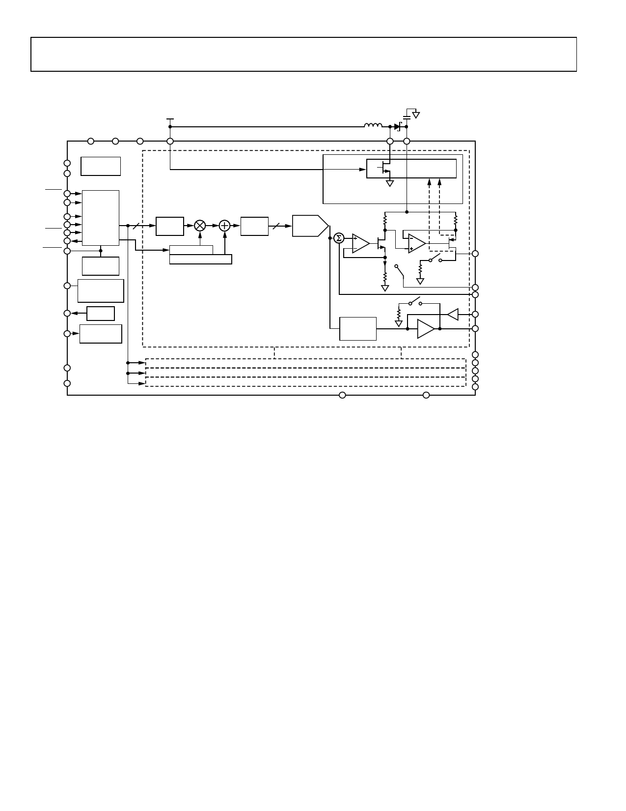
FUNCTIONAL BLOCK DIAGRAM
AVCC
5.0V
SWx
VBOOST_x
DVDD
DGND
LDAC
SCLK
SDIN
SYNC
SDO
CLEAR
FAULT
ALERT
AD1
AD0
REFOUT
REFIN
DIGITAL
INTERFACE
REFERENCE
AD5755-1
+
GAIN REG A
OFFSET REG A
DAC CHANNEL A
DAC CHANNEL B
DAC CHANNEL C
DAC CHANNEL D
DC-TO-DC
CONVERTER
7.4V TO 29.5V
DAC A
CURRENT AND
VOLTAGE
OUTPUT RANGE
SCALING
IOUT_x
RSET_x
CHARTx
+VSENSE_x
VOUT _x
NOTES
1. x = A, B, C, AND D.
Figure 1.
Rev. F
Document Feedback
Information furnished by Analog Devices is believed to be accurate and reliable. However, no
responsibility is assumed by Analog Devices for its use, nor for any infringements of patents or other
rights of third parties that may result from its use. Specifications subject to change without notice. No
license is granted by implication or otherwise under any patent or patent rights of Analog Devices.
Trademarksandregisteredtrademarksarethepropertyoftheirrespectiveowners.
One Technology Way, P.O. Box 9106, Norwood, MA 02062-9106, U.S.A.
Tel: 781.329.4700 ©2011–2014 Analog Devices, Inc. All rights reserved.
Technical Support
www.analog.com
1 page 
AD5755-1
Data Sheet
DETAILED FUNCTIONAL BLOCK DIAGRAM
AV CC
5.0V
AV SS
AV DD
–15V/0V AGND +15V
SWA
VBOOST_A
DVDD
DGND
LDAC
CLEAR
SCLK
SDIN
SYNC
SDO
FAULT
ALERT
REFOUT
REFIN
POWER-ON
RESET
INPUT
SHIFT
REGISTER
AND
CONTROL
16
STATUS
REGISTER
WATCHDOG
TIMER
(SPI ACTIVITY)
VREF
REFERENCE
BUFFERS
INPUT
REG A
GAIN REG A
OFFSET REG A
DAC CHANNEL A
AD1
AD5755-1
AD0
DAC CHANNEL B
DAC CHANNEL C
DAC CHANNEL D
DAC 16
REG A
DC-TO-DC
CONVERTER
POWER 7.4V TO 29.5V VSEN1
CONTROL
REG
VSEN2
DAC A
R2
R3
IOUT_A
R1
RSET_A
CHARTA
VOUT
RANGE
SCALING
30kΩ
+VSENSE_ A
VOUT_A
SWB, SWC, SWD
Figure 2.
IOUT_B, IOUT_C, IOUT_D
RSET_B, RSET_C, RSET_D
CHARTB, CHARTC, CHARTD
+VSENSE_B, +VSENSE_C, +VSENSE_D
VOUT_B, VOUT_C, VOUT_D
VBOOST_B, VBOOST_C, VBOOST_D
Rev. F | Page 4 of 51
5 Page 
AD5755-1
Timing Diagrams
SCLK
SYNC
SDIN
LDAC
VOUT_x
LDAC = 0
VOUT_x
CLEAR
VOUT_x
1
t6
t4
2
t7
MSB
t1
24
t3 t2
t5
t8
LSB
t10
t17
t19
t9 t10
t11
Data Sheet
t12
t13
t14
t12
t16
RESET
t18
Figure 3. Serial Interface Timing Diagram
SCLK
SYNC
1
24 1
t6
24
SDIN
MSB
LSB
MSB
LSB
SDO
INPUT WORD SPECIFIES
REGISTER TO BE READ
MSB
NOP CONDITION
LSB
UNDEFINED
SELECTED REGISTER DATA
t15 CLOCKED OUT
1IF FIRST SCLK IS NEGATIVE EDGE WITHIN SYNC FRAME OF NOP CONDITION, 7 DON’T CARE BITS + 16 DATA BITS CLOCKED OUT (TOTAL 23 BITS).
IF FIRST SCLK IS POSITIVE EDGE WITHIN SYNC FRAME OF NOP CONDITION, 8 DON’T CARE BITS + 16 DATA BITS CLOCKED OUT (TOTAL 24 BITS).
SEE THE READBACK OPERATION SECTION FOR FURTHER INFORMATION.
Figure 4. Readback Timing Diagram (Packet Error Checking Disabled)
Rev. F | Page 10 of 51
11 Page | ||
| Páginas | Total 30 Páginas | |
| PDF Descargar | [ Datasheet AD5755-1.PDF ] | |
Hoja de datos destacado
| Número de pieza | Descripción | Fabricantes |
| AD5755-1 | 4mA to 20mA and Voltage Output DAC | Analog Devices |
| Número de pieza | Descripción | Fabricantes |
| SLA6805M | High Voltage 3 phase Motor Driver IC. |
Sanken |
| SDC1742 | 12- and 14-Bit Hybrid Synchro / Resolver-to-Digital Converters. |
Analog Devices |
|
DataSheet.es es una pagina web que funciona como un repositorio de manuales o hoja de datos de muchos de los productos más populares, |
| DataSheet.es | 2020 | Privacy Policy | Contacto | Buscar |
