|
|
PDF CD4046BMS Data sheet ( Hoja de datos )
| Número de pieza | CD4046BMS | |
| Descripción | CMOS Micropower Phase Locked Loop | |
| Fabricantes | Intersil Corporation | |
| Logotipo |  |
|
Hay una vista previa y un enlace de descarga de CD4046BMS (archivo pdf) en la parte inferior de esta página. Total 11 Páginas | ||
|
No Preview Available !
CD4046BMS
December 1992
CMOS Micropower Phase Locked Loop
Features
• Very Low Power Consumption:
70µW (typ.) at VCO fo = 10kHz, VDD = 5V
• Operating Frequency Range Up to 1.4 MHz (typ.) at
VDD = 10V, RI = 5kΩ
• Low Frequency Drift: 0.04%/oC (typ.) at VDD = 10V
• Choice of Two Phase Comparators:
- Exclusive-OR Network (I)
- Edge-Controlled Memory Network with Phase-Pulse
Output for Lock Indication (II)
• High VCO Linearity: <1% (typ.) at VDD = 10V
• VCO Inhibit Control for ON-OFF Keying and Ultra-Low
Standby Power Consumption
• Source-Follower Output of VCO Control Input
(Demod. Output)
• Zener Diode to Assist Supply Regulation
• Standardize, Symmetrical Output Characteristics
• 100% Tested for Quiescent Current at 20V
• 5V, 10V and 15V Parametric Ratings
• Meets All Requirements of JEDEC Tentative Standard
No. 13B, “Standard Specifications for Description of ‘B’
Series CMOS Devices”
Applications
• FM Demodulator and Modulator
• Frequency Synthesis and Multiplication
• Frequency Discriminator
• Data Synchronization
• Voltage-to-Frequency Conversion
• Tone Decoding
• FSK - Modems
• Signal Conditioning
Description
CD4046BMS CMOS Micropower Phase-Locked Loop (PLL)
consists of a low power linear voltage-controlled oscillator (VCO)
and two different phase comparators having a common signal-
input amplifier and a common comparator input. A 5.2V zener
diode is provided for supply regulation if necessary.
The CD4046BMS is supplied in these 16-lead outline packages:
Braze Seal DIP H4W
Frit Seal DIP
H1F
Ceramic Flatpack H6W
VCO Section
The VCO requires one external capacitor C1 and one or two
external resistors (R1 or R1 and R2). Resistor R1 and capacitor
C1 determine the frequency range of the VCO and resistor R2
enables the VCO to have a frequency offset if required. The high
input impedance (1012Ω) of the VCO simplifies the design of low
pass filters by permitting the designer a wide choice of resistor-
to-capacitor ratios. In order not to load the low-pass filter, a
source-follower output of the VCO input voltage is provided at ter-
minal 10 (DEMODULATED OUTPUT). If this terminal is used, a
load resistor (RS) of 10kΩ or more should be connected from
this terminal to VSS. If unused this terminal should be left open.
The VCO can be connected either directly or through frequency
dividers to the comparator input of the phase comparators. A full
CMOS logic swing is available at the output of the VCO and
allows direct coupling to CMOS frequency dividers such as the
Intersil CD4024, CD4018, CD4020, CD4029, and CD4050. One
or more CD4018 (Preset Table Divide-By-N Counter) or CD4029
(Presettable Up/Down Counter) or CD4029 (Presettable Divide-
by-N Counter) or CD4029 (Presettable Up/Down Counter), or
CD4059A (Programmable Divide-by “N” Counter), together with
the CD4046BMS (Phase-Locked Loop) can be used to build a
micropower low-frequency synthesizer. A logic 0 on the INHIBIT
input “enables” the VCO and the source follower, while a logic 1
“turns off” both to minimize stand-by power consumption.
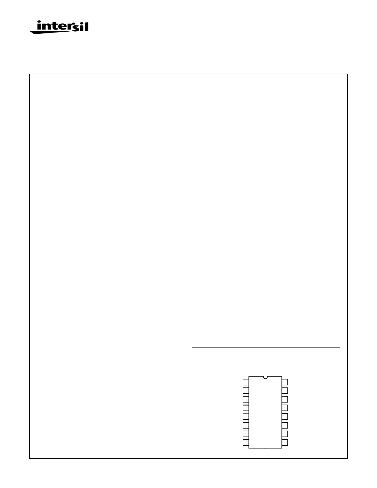
Pinout
CD4046BMS
TOP VIEW
PHASE PULSES 1
PHASE COMP I OUT 2
COMPARATOR IN 3
VCO OUT 4
INHIBIT 5
CI(1) 6
C1 (2) 7
VSS 8
16 VDD
15 ZENER
14 SIGNAL IN
13 PHASE COMP II OUT
12 R2 TO VSS
11 R1 TO VSS
10 DEMODULATOR OUT
9 VCO IN
CAUTION: These devices are sensitive to electrostatic discharge; follow proper IC Handling Procedures.
1-888-INTERSIL or 321-724-7143 | Copyright © Intersil Corporation 1999
7-886
File Number 3312
1 page 
Specifications CD4046BMS
TABLE 3. ELECTRICAL PERFORMANCE CHARACTERISTICS (Continued)
LIMITS
PARAMETER
SYMBOL
CONDITIONS
Quiescent Leakage
Phase Comparator
(Bias Amp Leakage)
BIAS LKG VDD = 5
VIN =
VDD or
GND
Pin 14 Open
Pin 5 = VDD
Pin 14 = VSS or VDD
Pin 5 = VDD
VDD = 10 Pin 14 Open
VIN =
Pin 5 = VDD
VDD or
GND
Pin 14 = VSS or VDD
Pin 5 = VDD
VDD = 15 Pin 14 Open
VIN =
Pin 5 = VDD
VDD or
GND
Pin 14 = VSS or VDD
Pin 5 = VDD
AC Coupled Signal In-
put Voltage Sensitivity
(Peak to Peak)
VS VDD = 10V, Input Frequency =
100kHz Sine Wave
VDD = 15V, Input Frequency =
100kHz Sine Wave
NOTES
1, 2
TEMPERATURE
+25oC/-55oC
MIN
-
1, 2 +25oC/-55oC -
1, 2 +25oC/-55oC -
1, 2 +25oC/-55oC -
1, 2 +25oC/-55oC -
1, 2 +25oC/-55oC -
1, 2 +25oC -
1, 2 +25oC -
MAX
0.2
UNITS
mA
20 µA
1.0 mA
40 µA
1.5 mA
80 µA
660 mV
1800
mV
NOTES:
1. All voltages referenced to device GND.
2. The parameters listed on Table 3 are controlled via design or process and are not directly tested. These parameters are characterized
on initial design release and upon design changes which would affect these characteristics.
TABLE 4. POST IRRADIATION ELECTRICAL PERFORMANCE CHARACTERISTICS
LIMITS
PARAMETER
SYMBOL
CONDITIONS
Supply Current
IDD VDD = 20V, VIN = VDD or GND
N Threshold Voltage
VNTH VDD = 10V, ISS = -10µA
N Threshold Voltage
Delta
∆VTN VDD = 10V, ISS = -10µA
P Threshold Voltage
VTP VSS = 0V, IDD = 10µA
P Threshold Voltage
Delta
∆VTP VSS = 0V, IDD = 10µA
Functional
F VDD = 18V, VIN = VDD or GND
VDD = 3V, VIN = VDD or GND
AC Coupled Signal Input
Voltage Sensitivity
VS VDD = 5V
Input Frequency = 100kHz
Sine Wave
NOTES
1, 4
1, 4
1, 4
1, 4
1, 4
1
1, 2, 3
TEMPERATURE
+25oC
+25oC
+25oC
MIN
-
-2.8
-
MAX
25
-0.2
±1
+25oC
+25oC
0.2 2.8
- ±1
+25oC
+25oC
VOH > VOL <
VDD/2 VDD/2
- 1.35 x
+25oC
Limit
NOTES: 1. All voltages referenced to device GND.
2. Go/No Go test with limits applied to inputs.
3. See Table 2 for +25oC limit.
UNITS
µA
V
V
V
V
V
mV
TABLE 5. BURN-IN AND LIFE TEST DELTA PARAMETERS +25OC
PARAMETER
SYMBOL
DELTA LIMIT
Supply Current - MSI-2
Output Current (Sink)
Output Current (Source)
IDD
IOL5
IOH5A
± 1.0µA
± 20% x Pre-Test Reading
± 20% x Pre-Test Reading
7-890
5 Page 
CD4046BMS
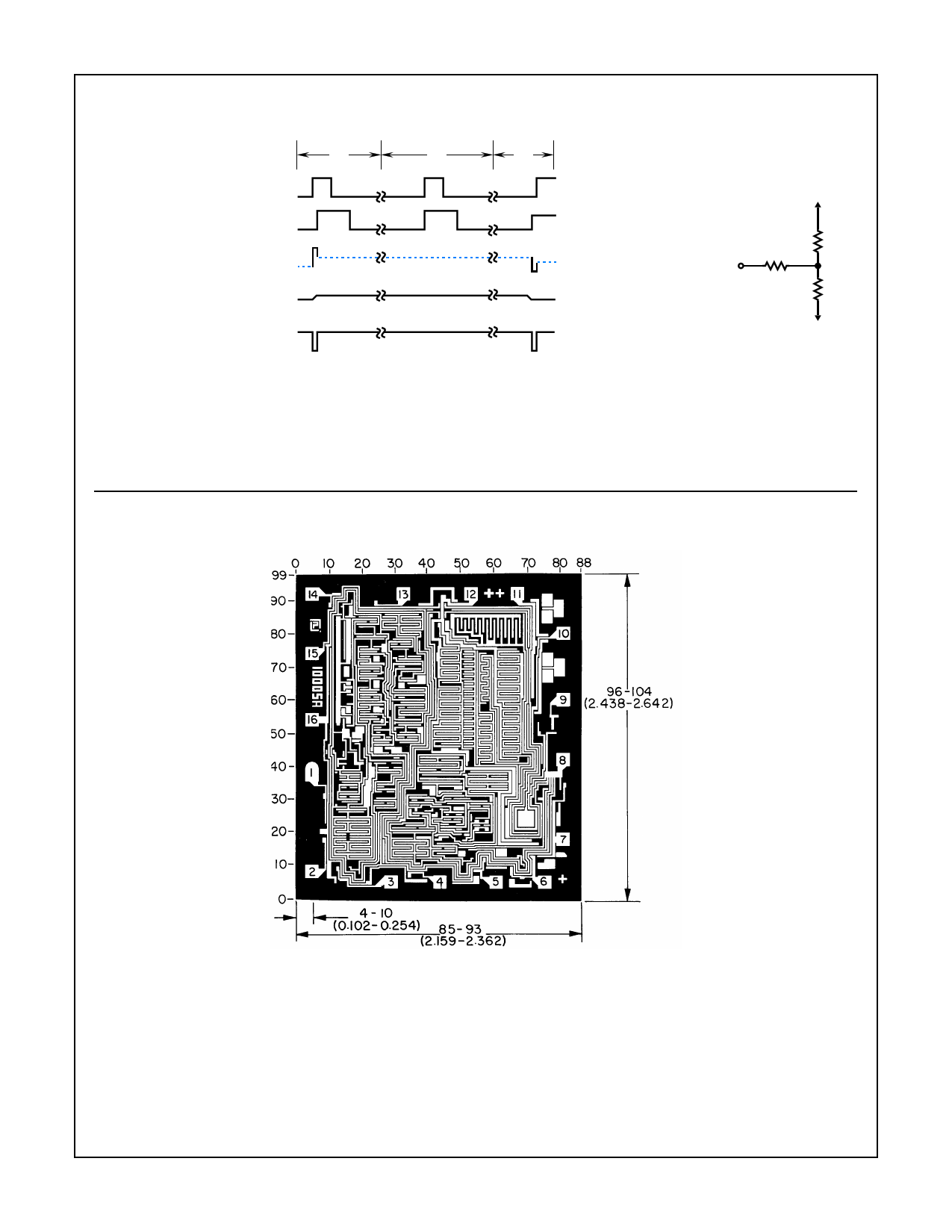
I II III
SIGNAL INPUT (TERM 14)
VCO OUTPUT (TERM 4) =
COMPARATOR INPUT (TERM 3)
PHASE COMPARATOR II
OUTPUT (TERM 13)
VCO INPUT (TERM 9) =
∆ LOW-PASS FILTER
OUTPUT
PHASE PULSE (TERM 1)
NOTE: DASHED LINE IS AN OPEN
CIRCUIT CONDITION
(3RD STATE)
-VDD
-VSS
-VDD
-VSS
-VDD
-VSS
FIGURE 15. TYPICAL WAVEFORMS FOR COS/MOS PHASE-LOCKED LOOP
EMPLOYING PHASE COMPARATOR II IN LOCKED CONDICTION
VDD
PHASE 13
COMPARATOR II
OUTPUT
20KΩ
2KΩ
2KΩ
VSS
FIGURE 16. PHASE COMPARATOR II
OUTPUT LOADING CIRCUIT
Chip Dimensions and Pad Layout
Dimensions in parentheses are in millimeters
and are derived from the basic inch dimensions
as indicated. Grid graduations are in mils (10-3 inch)
METALLIZATION: Thickness: 11kÅ − 14kÅ, AL.
PASSIVATION: 10.4kÅ - 15.6kÅ, Silane
BOND PADS: 0.004 inches X 0.004 inches MIN
DIE THICKNESS: 0.0198 inches - 0.0218 inches
7-896
11 Page | ||
| Páginas | Total 11 Páginas | |
| PDF Descargar | [ Datasheet CD4046BMS.PDF ] | |
Hoja de datos destacado
| Número de pieza | Descripción | Fabricantes |
| CD4046BM | Micropower Phase-Locked Loop | National Semiconductor |
| CD4046BMS | CMOS Micropower Phase Locked Loop | Intersil Corporation |
| Número de pieza | Descripción | Fabricantes |
| SLA6805M | High Voltage 3 phase Motor Driver IC. |
Sanken |
| SDC1742 | 12- and 14-Bit Hybrid Synchro / Resolver-to-Digital Converters. |
Analog Devices |
|
DataSheet.es es una pagina web que funciona como un repositorio de manuales o hoja de datos de muchos de los productos más populares, |
| DataSheet.es | 2020 | Privacy Policy | Contacto | Buscar |
