|
|
|
PDF AD7569 Data sheet ( Hoja de datos )
| Número de pieza | AD7569 | |
| Descripción | 8-Bit Analog I/0 Systems | |
| Fabricantes | Analog Devices | |
| Logotipo | ||
1. AD7569 Hay una vista previa y un enlace de descarga de AD7569 (archivo pdf) en la parte inferior de esta página. Total 20 Páginas | ||
|
No Preview Available !
a
FEATURES
2 s ADC with Track/Hold
1 s DAC with Output Amplifier
AD7569, Single DAC Output
AD7669, Dual DAC Output
On-Chip Bandgap Reference
Fast Bus Interface
Single or Dual 5 V Supplies
LC2MOS
Complete, 8-Bit Analog I/0 Systems
AD7569/AD7669
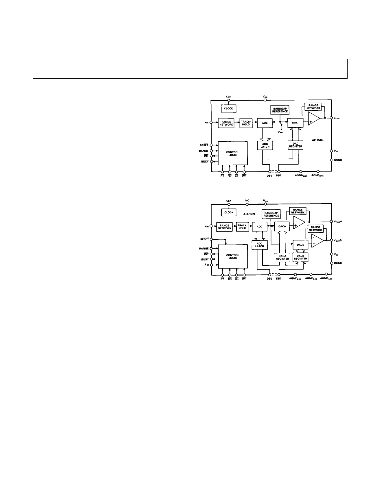
AD7569 FUNCTIONAL BLOCK DIAGRAM
GENERAL DESCRIPTION
The AD7569/AD7669 is a complete, 8-bit, analog I/O system
on a single monolithic chip. The AD7569 contains a high speed
successive approximation ADC with 2 µs conversion time, a track/
hold with 200 kHz bandwidth, a DAC and an output buffer ampli-
fier with 1 µs settling time. A temperature-compensated 1.25 V
bandgap reference provides a precision reference voltage for the
ADC and the DAC. The AD7669 is similar, but contains two
DACs with output buffer amplifiers.
A choice of analog input/output ranges is available. Using a sup-
ply voltage of +5 V, input and output ranges of zero to 1.25 V
and zero to 2.5 volts may be programmed using the RANGE in-
put pin. Using a ± 5 V supply, bipolar ranges of ± 1.25 V or
± 2.5 V may be programmed.
Digital interfacing is via an 8-bit I/O port and standard micro-
processor control lines. Bus interface timing is extremely fast, al-
lowing easy connection to all popular 8-bit microprocessors. A
separate start convert line controls the track/hold and ADC to
give precise control of the sampling period.
The AD7569/AD7669 is fabricated in Linear-Compatible
CMOS (LC2MOS), an advanced, mixed technology process
combining precision bipolar circuits with low power CMOS
logic. The AD7569 is packaged in a 24-pin, 0.3" wide “skinny”
DIP, a 24-terminal SOIC and 28-terminal PLCC and LCCC
packages. The AD7669 is available in a 28-pin, 0.6" plastic
DIP, 28-terminal SOIC and 28-terminal PLCC package.
AD7669 FUNCTIONAL BLOCK DIAGRAM
PRODUCT HIGHLIGHTS
1. Complete Analog I/O on a Single Chip.
The AD7569/AD7669 provides everything necessary to
interface a microprocessor to the analog world. No external
components or user trims are required and the overall accu-
racy of the system is tightly specified, eliminating the need
to calculate error budgets from individual component
specifications.
2. Dynamic Specifications for DSP Users.
In addition to the traditional ADC and DAC specifications,
the AD7569/AD7669 is specified for ac parameters, includ-
ing signal-to-noise ratio, distortion and input bandwidth.
3. Fast Microprocessor Interface.
The AD7569/AD7669 has bus interface timing compatible
with all modern microprocessors, with bus access and relin-
quish times less than 75 ns and write pulse width less than
80 ns.
REV. B
Information furnished by Analog Devices is believed to be accurate and
reliable. However, no responsibility is assumed by Analog Devices for its
use, nor for any infringements of patents or other rights of third parties
which may result from its use. No license is granted by implication or
otherwise under any patent or patent rights of Analog Devices.
One Technology Way, P.O. Box 9106, Norwood, MA 02062-9106, U.S.A.
Tel: 617/329-4700
World Wide Web Site: http://www.analog.com
Fax: 617/326-8703
© Analog Devices, Inc., 1996
1 page 
AD7569/AD7669
NOTE:
The term DAC (Digital-to-Analog Converter) throughout the
data sheet applies equally to the dual DACs in the AD7669 as
well as to the single DAC of the AD7569 unless otherwise
stated. It follows that the term VOUT applies to both VOUTA and
VOUTB of the AD7669 also.
TERMINOLOGY
Total Unadjusted Error
Total unadjusted error is a comprehensive specification that in-
cludes internal voltage reference error, relative accuracy, gain
and offset errors.
Relative Accuracy (DAC)
Relative Accuracy or endpoint nonlinearity is a measure of the
maximum deviation from a straight line passing through the
endpoints of the DAC transfer function. It is measured after al-
lowing for offset and gain errors. For the bipolar output ranges,
the endpoints of the DAC transfer function are defined as those
voltages that correspond to negative full-scale and positive full-
scale codes. For the unipolar output ranges, the endpoints are
code 1 and code 255. Code 1 is chosen because the amplifier is
now working in single supply and, in cases where the true offset
of the amplifier is negative, it cannot be seen at code 0. If the
relative accuracy were calculated between code 0 and code 255,
the “negative offset” would appear as a linearity error. If the off-
set is negative and less than 1 LSB, it will appear at code 1, and
hence the true linearity of the converter is seen between code 1
and code 255.
Relative Accuracy (ADC)
Relative Accuracy is the deviation of the ADC’s actual code
transition points from a straight line drawn between the end-
points of the ADC transfer function. For the bipolar input
ranges, these points are the measured, negative, full-scale transi-
tion point and the measured, positive, full-scale transition point.
For the unipolar ranges, the straight line is drawn between the
measured first LSB transition point and the measured full-scale
transition point.
Differential Nonlinearity
Differential Nonlinearity is the difference between the measured
change and an ideal 1 LSB change between any two adjacent
codes. A specified differential nonlinearity of ± 1 LSB max en-
sures monotonicity (DAC) or no missed codes (ADC). A differ-
ential nonlinearity of ± 3/4 LSB max ensures that the minimum
step size (DAC) or code width (ADC) is 1/4 LSB, and the maxi-
mum step size or code width is 3/4 LSB.
Digital-to-Analog Glitch Impulse
Digital-to-Analog Glitch Impulse is the impulse injected into the
analog output when the digital inputs change state with the
DAC selected. It is normally specified as the area of the glitch in
nV secs and is measured when the digital input code is changed
by 1 LSB at the major carry transition.
Digital Feedthrough
Digital Feedthrough is also a measure of the impulse injected to
the analog output from the digital inputs, but is measured when
the DAC is not selected. It is essentially feedthrough across the
die and package. It is also a measure of the glitch impulse trans-
ferred to the analog output when data is read from the internal
ADC. It is specified in nV secs and is measured with WR high
and a digital code change from all 0s to all 1s.
DAC-to-DAC Crosstalk (AD7669 Only)
The glitch energy transferred to the output of one DAC due to
an update at the output of the second DAC. The figure given is
the worst case and is expressed in nV secs. It is measured with
an update voltage of full scale.
DAC-to-DAC Isolation (AD7669 Only)
DAC-to-DAC Isolation is the proportion of a digitized sine
wave from the output of one DAC, which appears at the output
of the second DAC (loaded with all 1s). The figure given is the
worst case for the second DAC output and is expressed as a ra-
tio in dBs. It is measured with a digitized sine wave (fSAMPLING =
100 kHz) of 20 kHz at 2.5 V pk-pk.
Signal-to-Noise Ratio
Signal-to-Noise Ratio (SNR) is the measured signal to noise at
the output of the converter. The signal is the rms magnitude of
the fundamental. Noise is the rms sum of all the nonfundamen-
tal signals (excluding dc) up to half the sampling frequency.
SNR is dependent on the number of quantization levels used in
the digitization process; the more levels, the smaller the quanti-
zation noise. The theoretical SNR for a sine wave is given by
SNR = (6.02N + 1.76) dB
where N is the number of bits. Thus for an ideal 8-bit converter,
SNR = 50 dB.
Harmonic Distortion
Harmonic Distortion is the ratio of the rms sum of harmonics to
the fundamental. For the AD7569/AD7669, Total Harmonic
Distortion (THD) is defined as
20 log
V
2
2
+
V
2
3
+
V
2
4
+V
2
5
+V
2
6
V1
where V1 is the rms amplitude of the fundamental and V2, V3,
V4, V5 and V6 are the rms amplitudes of the individual
harmonics.
Intermodulation Distortion
With inputs consisting of sine waves at two frequencies, fa and
fb, any active device with nonlinearities will create distortion
products, of order (m + n), at sum and difference frequencies of
mfa ± nfb where m, n = 0, l, 2, 3,… . Intermodulation terms
are those for which m or n is not equal to zero. For example,
the second order terms include (fa + fb) and (fa – fb) and the
third order terms include (2fa + fb), (2fa – fb), (fa + 2fb) and
(fa – 2fb).
REV. B
–5–
5 Page 
RESET line, the DAC output resets to 0 V when the entire
system is reset. Figure 7 shows the input control logic for the
AD7569 DAC; the write cycle timing diagram is shown in
Figure 8.
AD7569/AD7669
The contents of the DAC registers are reset to all 0s by an active
low pulse on the RESET line, and for the unipolar output
ranges, the outputs remain at 0 V after RESET returns high.
For the bipolar output ranges, a low pulse on RESET causes the
outputs to go to negative full scale. In unipolar applications, the
RESET line can be used to ensure power-up to 0 V on the
AD7669 DAC outputs and is also useful when used as a zero
override in system calibration cycles. If the RESET input is con-
nected to the system RESET line, then the DAC outputs reset
to 0 V when the entire system is reset. Figure 9 shows the DAC
input control logic for the AD7669, and the write cycle timing
diagram is shown in Figure 8.
Figure 7. AD7569 DAC Input Control Logic
Figure 9. AD7669 DAC Control Logic
Figure 8. AD7569/AD7669 Write Cycle Timing Diagram
DAC Timing and Control—AD7669
Table III shows the truth table for the dual DAC operation of
the AD7669. The part contains two 8-bit DAC registers that are
loaded from the data bus under the control of CS, A/B and WR.
Address line A/B selects which DAC register the data is
loaded to. The data contained in the DAC registers determines
the analog output from the respective DACs. The WR input is
an edge-triggered input, and data is transferred into the selected
DAC register on the rising edge of WR. Holding CS and WR
low does not make the selected DAC register transparent. The
A/B input should not be changed while CS and WR are low.
ADC Timing and Control
The ADC on the AD7569/AD7669 is capable of two basic oper-
ating modes. In the first mode, the ST line is used to start con-
version and drive the track-and-hold into hold mode. At the end
of conversion, the track-and-hold returns to its tracking mode.
The second mode is achieved by hard-wiring the ST line high.
In this case, CS and RD start conversion, and the microproces-
sor is driven into a WAIT state for the duration of conversion by
BUSY.
Table III. AD7669 DAC Truth Table
CS WR A/B RESET DAC Function
HH
Lg
gL
Lg
gL
XX
X
L
L
H
H
X
H
H
H
H
H
L
DAC Registers Unaffected
DACA Register Updated
DACA Register Updated
DACB Register Updated
DACB Register Updated
DAC Registers Loaded with
All Zeros
L = Low State, H = High State, X = Don’t Care
REV. B
–11–
Figure 10. ADC Mode 1 Interface Timing
11 Page | ||
| Páginas | Total 20 Páginas | |
| PDF Descargar | [ Datasheet AD7569.PDF ] | |
Hoja de datos destacado
| Número de pieza | Descripción | Fabricantes |
| AD7564 | LC2MOS +3.3 V/+5 V/ Low Power/ Quad 12-Bit DAC | Analog Devices |
| AD7568 | LC2MOS Octal 12-Bit DAC | Analog Devices |
| AD7569 | 8-Bit Analog I/0 Systems | Analog Devices |
| Número de pieza | Descripción | Fabricantes |
| SLA6805M | High Voltage 3 phase Motor Driver IC. |
Sanken |
| SDC1742 | 12- and 14-Bit Hybrid Synchro / Resolver-to-Digital Converters. |
Analog Devices |
|
DataSheet.es es una pagina web que funciona como un repositorio de manuales o hoja de datos de muchos de los productos más populares, |
| DataSheet.es | 2020 | Privacy Policy | Contacto | Buscar |