|
|
|
PDF AD9363 Data sheet ( Hoja de datos )
| Número de pieza | AD9363 | |
| Descripción | RF Agile Transceiver | |
| Fabricantes | Analog Devices | |
| Logotipo | ||
Hay una vista previa y un enlace de descarga de AD9363 (archivo pdf) en la parte inferior de esta página. Total 30 Páginas | ||
|
No Preview Available !
Data Sheet
FEATURES
Radio frequency (RF) 2 × 2 transceiver with integrated 12-bit
DACs and ADCs
Wide bandwidth: 325 MHz to 3.8 GHz
Supports time division duplex (TDD) and frequency division
duplex (FDD) operation
Tunable channel bandwidth (BW): up to 20 MHz
Receivers: 6 differential or 12 single-ended inputs
Superior receiver sensitivity with a noise figure: 3 dB
Receive (Rx) gain control
Real-time monitor and control signals for manual gain
Independent automatic gain control (AGC)
Dual transmitters: 4 differential outputs
Highly linear broadband transmitter
Transmit (Tx) error vector magnitude (EVM): −34 dB
Tx noise: ≤−157 dBm/Hz noise floor
Tx monitor: 66 dB dynamic range with 1 dB accuracy
Integrated fractional N synthesizers
2.4 Hz local oscillator (LO) step size
CMOS/LVDS digital interface
APPLICATIONS
3G enterprise femtocell base stations
4G femtocell base stations
Wireless video transmission
GENERAL DESCRIPTION
The AD9363 is a high performance, highly integrated RF agile
transceiver designed for use in 3G and 4G femtocell applications.
Its programmability and wideband capability make it ideal for a
broad range of transceiver applications. The device combines an
RF front end with a flexible mixed-signal baseband section and
integrated frequency synthesizers, simplifying design-in by
providing a configurable digital interface to a processor. The
AD9363 operates in the 325 MHz to 3.8 GHz range, covering
most licensed and unlicensed bands. Channel bandwidths from
less than 200 kHz to 20 MHz are supported.
The two independent direct conversion receivers have state-of-
the-art noise figure and linearity. Each Rx subsystem includes
independent automatic gain control (AGC), dc offset correction,
quadrature correction, and digital filtering, thereby eliminating
the need for these functions in the digital baseband. The AD9363
also has flexible manual gain modes that can be externally
controlled. Two high dynamic range ADCs per channel digitize
the received I and Q signals and pass them through configurable
decimation filters and 128-tap finite impulse response (FIR)
filters to produce a 12-bit output signal at the appropriate
Rev. D
Document Feedback
Information furnished by Analog Devices is believed to be accurate and reliable. However, no
responsibilityisassumedbyAnalogDevices for itsuse,nor foranyinfringementsofpatentsor other
rights of third parties that may result from its use. Specifications subject to change without notice. No
license is granted by implication or otherwise under any patent or patent rights of Analog Devices.
Trademarksandregisteredtrademarksarethepropertyoftheirrespectiveowners.
RF Agile Transceiver
AD9363
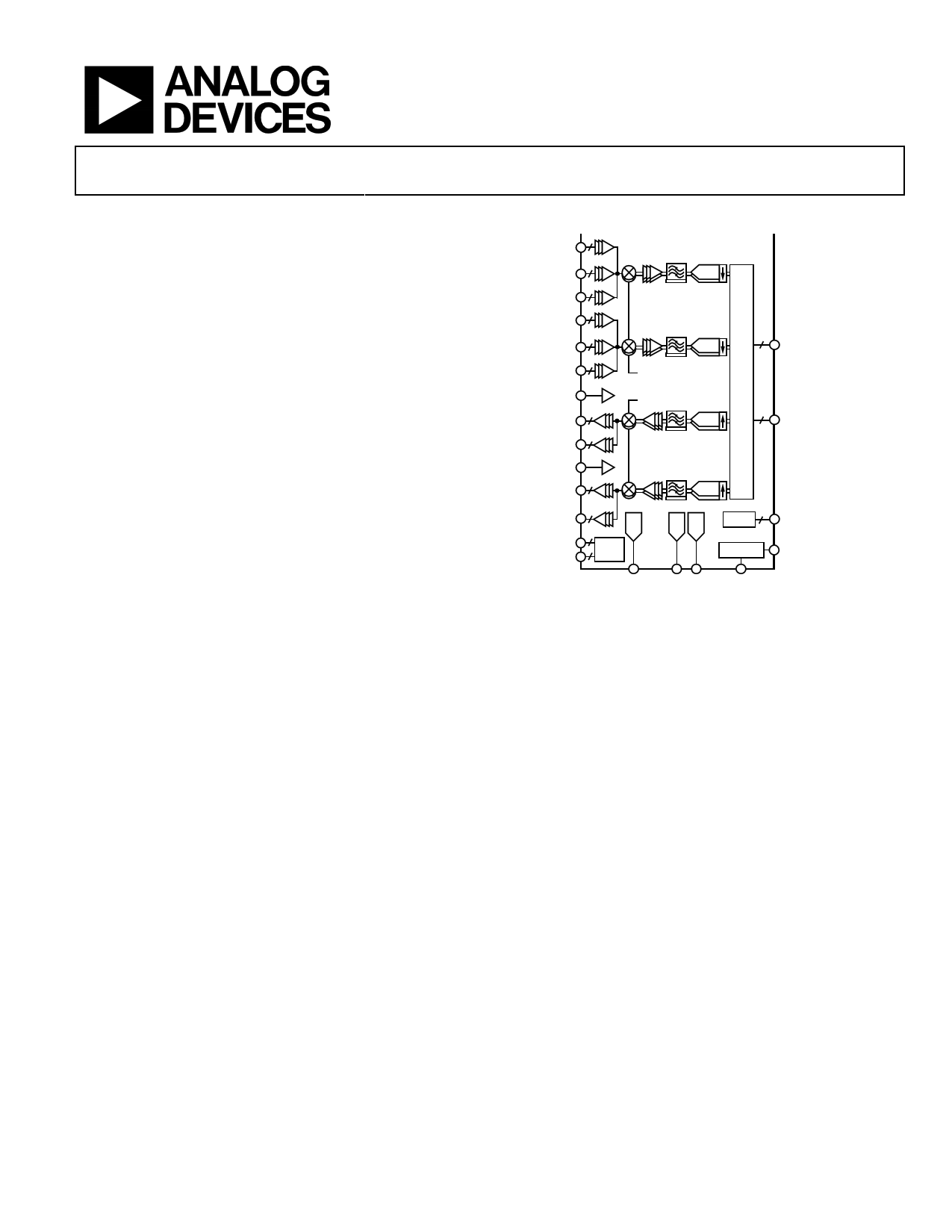
FUNCTIONAL BLOCK DIAGRAM
RX1B_P,
RX1B_N
RX1A_P,
RX1A_N
RX1C_P,
RX1C_N
RX2B_P,
RX2B_N
RX2A_P,
RX2A_N
RX2C_P,
RX2C_N
AD9363
ADC
RX LO
ADC
P0_D11/
TX_D5_x TO P0_D0/
TX_D0_x
TX_MON1
TX1A_P,
TX1A_N
TX1B_P,
TX1B_N
TX_MON2
TX2A_P,
TX2A_N
TX2B_P,
TX2B_N
SPI
CTRL
TX LO
CTRL
DAC
DAC
GPO
PLLs
P1_D11/
RX_D5_x TO P1_D0/
RX_D0_x
RADIO
SWITCHING
CLK_OUT
AUXADC AUXDACx XTALN
NOTES
1. SPI, CTRL, P0_D11/TX_D5_x TO P0_D0/TX_D0_x, P1_D11/
RX_D5_x TO P1_D0/RX_D0_x, AND RADIO SWITCHING
CONTAIN MULTIPLE PINS.
Figure 1.
sample rate.
The transmitters use a direct conversion architecture that achieves
high modulation accuracy with ultralow noise. This transmitter
design produces a best-in-class Tx EVM of −34 dB, allowing
significant system margin for the external power amplifier (PA)
selection. The on-board Tx power monitor can be used as a
power detector, enabling highly accurate Tx power
measurements.
The fully integrated phase-locked loops (PLLs) provide low
power fractional N frequency synthesis for all receive and
transmit channels. Channel isolation, demanded by FDD
systems, is integrated into the design. All voltage controlled
oscillators (VCOs) and loop filter components are integrated.
The core of the AD9363 can be powered directly from a 1.3 V
regulator. The IC is controlled via a standard 4-wire serial port
and four real-time I/O control pins. Comprehensive power-down
modes are included to minimize power consumption during
normal use. The AD9363 is packaged in a 10 mm × 10 mm,
144-ball chip scale package ball grid array (CSP_BGA).
One Technology Way, P.O. Box 9106, Norwood, MA 02062-9106, U.S.A.
Tel: 781.329.4700
©2016 Analog Devices, Inc. All rights reserved.
Technical Support
www.analog.com
1 page 
Data Sheet
AD9363
Parameter1
Third-Order Output Intermodulation
Intercept Point
Carrier Leakage
Noise Floor
Isolation
TX1 to TX2
TX2 to TX1
Symbol Min Typ
OIP3
18
Max Unit
dBm
Test Conditions/Comments
−50
−31
−154
dBc 0 dB attenuation
dBc 40 dB attenuation
dBm/Hz 90 MHz offset
50 dB
50 dB
1 When referencing a single function of a multifunction pin in the parameters, only the portion of the pin name that is relevant to the specification is listed. For full pin
names of multifunction pins, refer to the Pin Configuration and Function Descriptions section.
Table 2.
Parameter1
TX MONITOR INPUTS
(TX_MON1, TX_MON2)
Maximum Input Level
Dynamic Range
Accuracy
LO SYNTHESIZER
LO Frequency Step
Integrated Phase Noise
REFERENCE CLOCK (REF_CLK)
Input Frequency Range
Input Signal Level
AUXILIARY ADC
Resolution
Input Voltage
Minimum
Maximum
AUXILIARY DAC
Resolution
Output Voltage
Minimum
Maximum
Output Current
DIGITAL SPECIFICATIONS
(CMOS)
Logic Inputs
Input Voltage High
Input Voltage Low
Input Current High
Input Current Low
Logic Outputs
Output Voltage High
Output Voltage Low
DIGITAL SPECIFICATIONS (LVDS)
Logic Inputs
Input Voltage Range
Input Differential Voltage
Threshold
Symbol Min
10
Typ
4
66
1
2.4
0.3
1.3
12
0.05
VDDA1P3_BB −
0.05
10
0.5
VDD_GPO − 0.3
10
VDD_INTERFACE ×
0.8
0
−10
−10
VDD_INTERFACE ×
0.8
0
825
−100
Rev. D | Page 5 of 32
Max Unit Test Conditions/Comments
dBm
dB
dB
Hz 2.4 GHz, 40 MHz reference clock
°rms 100 Hz to 100 MHz
REF_CLK is the input to the
XTALN pin
80 MHz External oscillator
V p-p AC-coupled external oscillator
Bits
V
V
Bits
V
V
mA
VDD_INTERFACE V
VDD_INTERFACE ×
0.2
+10
+10
V
μA
μA
VDD_INTERFACE V
VDD_INTERFACE × V
0.2
1575
+100
mV Each differential input in the
pair
mV
5 Page 
Data Sheet
AD9363
CURRENT CONSUMPTION—VDDx (COMBINATION OF ALL 1.3 V SUPPLIES)
Table 6. TDD Mode, 800 MHz
Parameter
ONE Rx CHANNEL
5 MHz BW
10 MHz BW
20 MHz BW
TWO Rx CHANNELS
5 MHz BW
10 MHz BW
20 MHz BW
ONE Tx CHANNEL
5 MHz BW
7 dBm
−27 dBm
10 MHz BW
7 dBm
−27 dBm
20 MHz BW
7 dBm
−27 dBm
TWO Tx CHANNELS
5 MHz BW
7 dBm
−27 dBm
10 MHz BW
7 dBm
−27 dBm
20 MHz BW
7 dBm
−27 dBm
Min Typ Max Unit Test Conditions/Comments
Continuous Rx
180 mA
210 mA
260 mA
Continuous Rx
265 mA
315 mA
405 mA
Continuous Tx
340 mA
190 mA
360 mA
220 mA
400 mA
250 mA
Continuous Tx
550 mA
260 mA
600 mA
310 mA
660 mA
370 mA
Rev. D | Page 11 of 32
11 Page | ||
| Páginas | Total 30 Páginas | |
| PDF Descargar | [ Datasheet AD9363.PDF ] | |
Hoja de datos destacado
| Número de pieza | Descripción | Fabricantes |
| AD9361 | RF Agile Transceiver | Analog Devices |
| AD9363 | RF Agile Transceiver | Analog Devices |
| AD9364 | RF Agile Transceiver | Analog Devices |
| Número de pieza | Descripción | Fabricantes |
| SLA6805M | High Voltage 3 phase Motor Driver IC. |
Sanken |
| SDC1742 | 12- and 14-Bit Hybrid Synchro / Resolver-to-Digital Converters. |
Analog Devices |
|
DataSheet.es es una pagina web que funciona como un repositorio de manuales o hoja de datos de muchos de los productos más populares, |
| DataSheet.es | 2020 | Privacy Policy | Contacto | Buscar |