|
|
|
PDF AD9576 Data sheet ( Hoja de datos )
| Número de pieza | AD9576 | |
| Descripción | Asynchronous Clock Generator | |
| Fabricantes | Analog Devices | |
| Logotipo | ||
Hay una vista previa y un enlace de descarga de AD9576 (archivo pdf) en la parte inferior de esta página. Total 30 Páginas | ||
|
No Preview Available !
Data Sheet
FEATURES
Single, low phase noise, fully integrated VCO/fractional-N
PLL core
VCO range: 2375 MHz to 2725 MHz
Integrated loop filter (requires a single external capacitor)
2 differential, XTAL, or single-ended reference inputs
Reference monitoring capability
Automatic redundant XTAL switchover
Minimal transient, smooth switching
Typical RMS jitter
<0.3 ps (12 kHz to 20 MHz), integer-N translations
<0.5 ps (12 kHz to 20 MHz), fractional-N translations
Input frequency
8 kHz, 1.544 MHz, 2.048 MHz, and 10 MHz to 325 MHz
Preset frequency translations via pin strapping (PPRx)
Using a 25 MHz input reference
24.576 MHz, 25 MHz, 33.33 MHz, 50 MHz, 70.656 MHz,
100 MHz, 125 MHz, 148.5 MHz, 156.25 MHz,
161.1328 MHz, 312.5 MHz, 322.2656 MHz, 625 MHz,
or 644.5313 MHz
Using a 19.44 MHz input reference
50 MHz, 100 MHz, 125 MHz, 156.25 MHz, 161.1328 MHz,
or 644.5313 MHz
Using a 30.72 MHz input reference
25 MHz, 50 MHz, 100 MHz, 125 MHz, or 156.25 MHz
Single, general-purpose, fully integrated VCO/integer-N
PLL core
VCO range: 750 MHz to 825 MHz
Integrated loop filter
Independent, duplicate reference input or operation from
the fractional-N PLL active reference input
Input frequency: 25 MHz
Preset frequency translations via pin strapping (PPRx)
25 MHz, 33.33 MHz, 50 MHz, 66.67 MHz, 100 MHz,
133.33 MHz, 200 MHz, or 400 MHz
Up to 3 copies of reference clock output
11 pairs of configurable differential outputs
Output drive formats
3 outputs: HSTL, LVDS, HCSL, 1.8 V CMOS, 2.5 V/3.3 V CMOS
8 outputs: HSTL, LVDS, or 1.8 V CMOS
2.5 V or 3.3 V single-supply operation
APPLICATIONS
Ethernet line cards, switches, and routers
Baseband units
SATA and PCI express
Low jitter, low phase noise clock generation
Asynchronous clock generation
Rev. 0
Document Feedback
Information furnished by Analog Devices is believed to be accurate and reliable. However, no
responsibility is assumed by Analog Devices for its use, nor for any infringements of patents or other
rights of third parties that may result from its use. Specifications subject to change without notice. No
license is granted by implication or otherwise under any patent or patent rights of Analog Devices.
Trademarksandregisteredtrademarksarethepropertyoftheirrespectiveowners.
Dual PLL,
Asynchronous Clock Generator
AD9576
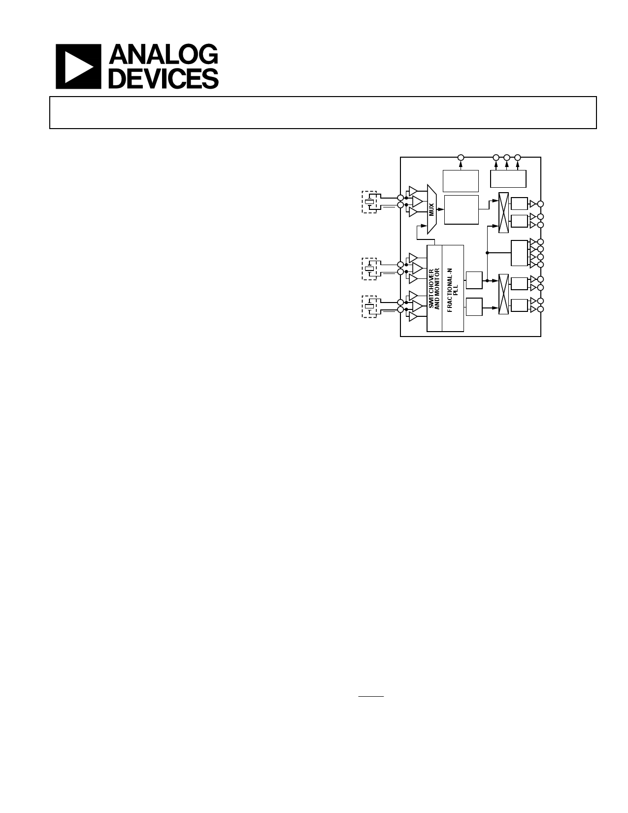
FUNCTIONAL BLOCK DIAGRAM
OPTIONAL
REF2
REF2
SPI/I2C
AND PPRx
CONTROL
GENERAL-
PURPOSE
PLL
STATUS
MONITOR
DIV
DIV
OUT10
OUT9
OUT8
OPTIONAL
REF0
REF0
OPTIONAL
REF1
REF1
VCO
DIV
VCO
DIV
DIV
DIV
DIV
AD9576
OUT0
OUT1
OUT2
OUT3
OUT4
OUT5
OUT6
OUT7
Figure 1.
GENERAL DESCRIPTION
The AD9576 provides a multiple output clock generator
function comprising two dedicated phase-locked loop (PLL)
cores with flexible frequency translation capability, optimized to
serve as a robust source of asynchronous clocks for an entire
system, providing extended operating life within frequency
tolerance through monitoring of and automatic switchover
between redundant crystal (XTAL) inputs with minimized
switching, induced transients. The fractional-N PLL design is
based on the Analog Devices, Inc., proven portfolio of high
performance, low jitter frequency synthesizers to maximize
network performance, whereas the integer-N PLL provides
general-purpose clocks for use as CPU and field-programmable
gate array (FPGA) reference clocks.
The AD9576 uses pin strapping to select among a multitude of
power-on ready configurations for its 11 output clocks, which
require only the connection of external pull-up or pull-down
resistors to the appropriate pin program reader pins (PPRx).
These pins provide control of the internal dividers for establishing
the desired frequency translations, clock output functionality,
and input reference functionality. These parameters can also be
manually configured through a serial port interface (SPI).
The AD9576 is packaged in a 64-lead, 9 mm × 9 mm LFCSP,
requiring only a single 2.5 V or 3.3 V supply. The operating
temperature range is −40°C to +85°C.
Each OUTx output is differential and contains two pins: OUTx
and OUTx. For simplicity, the term OUTx refers to the
functional output block containing these two pins.
One Technology Way, P.O. Box 9106, Norwood, MA 02062-9106, U.S.A.
Tel: 781.329.4700
©2016 Analog Devices, Inc. All rights reserved.
Technical Support
www.analog.com
1 page 
AD9576
Data Sheet
Parameter
1.8 V CMOS
VDD_OUT67 (Pin 29)
VDD_OUT45 (Pin 35)
VDD_OUT23 (Pin 41)
VDD_OUT01(Pin 46)
VDD_OUT89 (Pin 52)
VDD_OUT10 (Pin 57)
2.5 V CMOS
VDD_OUT89 (Pin 52)
VDD_OUT10 (Pin 57)
3.3 V CMOS
VDD_OUT89 (Pin 52)
VDD_OUT10 (Pin 57)
High Speed Current Sinking
Logic (HCSL)
VDD_OUT89 (Pin 52)
VDD_OUT10 (Pin 57)
Min Typ Max Unit
27.2 34.7
27.2 34.7
28.2 31.7
17.4 21.9
32.7 42.5
21.4 26.8
mA
mA
mA
mA
mA
mA
38.5 48.8
24.4 30.1
mA
mA
48.5 60.4
29.1 36.2
mA
mA
30.7 41.4
20.8 26.6
mA
mA
Test Conditions/Comments
All outputs at 100 MHz with a 10 pF load
VDD_x set to 2.5 V, output at 100 MHz with a 10 pF load; not
available on OUT0 to OUT7
VDD_x set to 3.3 V, all outputs at 100 MHz with a 10 pF load; not
available on OUT0 to OUT7
All outputs at 400 MHz; not available on OUT0 to OUT7
POWER DISSIPATION SPECIFICATIONS
Table 3.
Parameter
POWER DISSIPATION
Min Typ Max Unit
Typical Configuration 1
680 1168 mW
Typical Configuration 2
619 974 mW
All Blocks Running
979 1520 mW
Minimal Power
Configuration
INCREMENTAL POWER
DISSIPATION
Input Reference On/Off
Single-Ended
Differential
Output Driver On/Off
LVDS at 156.25 MHz
HSTL at 156.25 MHz
1.8 V CMOS at
100 MHz
2.5 V CMOS at
100 MHz
145 179 mW
2.5 10
27.5 33.7
mW
mW
47.6 66.1
51.3 80.8
64.6 74.1
mW
mW
mW
88.4 102.5 mW
Test Conditions/Comments
All supplies set to 2.5 V nominal; specifications do not include power
dissipated by external terminations
Asynchronous operation; PPR0 = State 0, PPR1 = State 0, PPR2 = State 3,
PPR3 = State 3; REF 0 and REF1 = 25 MHz XTAL, doubler enabled; OUT10 =
25 MHz CMOS; OUT0 to OUT3 = 100 MHz LVDS; OUT4 to OUT5 = 312.5 MHz
LVDS, OUT6 to OUT7 = 156.25 MHz LVDS, OUT8 to OUT9 = 125 MHz LVDS
Synchronous operation; REF0 (differential) at 100 MHz, REF1 disabled, and
REF2 (XTAL) at 25 MHz; PLL1 disabled and PLL0 locked at 2500 MHz using R
divider of 2 and PLL0 feedback divider (N0) set to 50; M0 and M1 set to
divide by 2; Output 0 set to 625 MHz HSTL; Output 1 to Output 3 disabled;
Output 4 to Output 7 set to 125 MHz LVDS; Output 8 to Output 9 set to
156.25 MHz LVDS
All blocks running; REF0 (differential) and REF1 (differential) at 300 MHz;
PLL0 locked at 2500 MHz with a 100 MHz PFD rate; M0 set to 2 and enabled to
Q0, Q1, and Q2; OUT0 to OUT3 = 625 MHz LVDS; OUT4 to OUT 7 = 1250 MHz
LVDS; REF2 (XTAL) at 25 MHz, configured as PLL1 input; PLL1 locked to
800 MHz with input doubler enabled; Divider Q3 and Divider Q4 set to 2 and
OUT8 to OUT10 = 400 MHz, HCSL
PPR0 = State 0, PPR1 = State 0, PPR2 = State 0, PPR3 = State 0
Typical configuration; values show the change in power due to the indicated
operation
Applies to one reference clock input at 25 MHz
A single 1.8 V CMOS output with a 10 pF load
A single 2.5 V CMOS output with a 10 pF load
Rev. 0 | Page 4 of 64
5 Page 
AD9576
Data Sheet
PLL0 CHANNELS ABSOLUTE CLOCK JITTER SPECIFICATIONS
Reference input frequency source is a 25 MHz Taitien XTAL, and frequency multiplier (×2) at PLL input enabled, unless otherwise noted.
Table 10.
Parameter
HSTL INTEGRATED RMS JITTER
Jitter Integration Bandwidth = 10 kHz to 10 MHz
Integer-N Translations
100 MHz Output
125 MHz Output
156.25 MHz Output
625 MHz Output
Fractional-N Translations
70.656 MHz Output
148.5 MHz Output
153.6 MHz Output
644.53125 MHz Output
Jitter Integration Bandwidth = 12 kHz to 20 MHz
Integer-N Translations
100 MHz Output
125 MHz Output
156.25 MHz Output
625 MHz Output
Fractional-N Translations
70.656 MHz Output
148.5 MHz Output
153.6 MHz Output
644.53125 MHz Output
Jitter Integration Bandwidth = 50 kHz to 80 MHz
312.5 MHz Output
Jitter Integration Bandwidth = 1.875 MHz to 20 MHz
Integer-N Translations
100 MHz Output
125 MHz Output
156.25 MHz Output
625 MHz Output
Fractional-N Translations
70.656 MHz Output
148.5 MHz Output
153.6 MHz Output
644.53125 MHz Output
LVDS INTEGRATED RMS JITTER
Jitter Integration Bandwidth = 10 kHz to 10 MHz
Integer-N Translations
100 MHz Output
125 MHz Output
156.25 MHz Output
625 MHz Output
Fractional-N Translations
70.656 MHz Output
148.5 MHz Output
153.6 MHz Output
644.53125 MHz Output
Min Typ Max Unit Test Conditions/Comments
0.233
0.218
0.218
0.221
0.291
0.307
0.292
0.313
0.239
0.222
0.221
0.222
0.298
0.310
0.296
0.314
0.237
0.088
0.076
0.071
0.053
0.119
0.106
0.103
0.096
ps
ps
ps
ps
ps
ps
ps
ps
ps
ps
ps
ps
ps
ps
ps
ps
ps
ps
ps
ps
ps
ps
ps
ps
ps
0.242
0.227
0.250
0.221
0.351
0.329
0.327
0.313
ps
ps
ps
ps
ps
ps
ps
ps
Rev. 0 | Page 10 of 64
11 Page | ||
| Páginas | Total 30 Páginas | |
| PDF Descargar | [ Datasheet AD9576.PDF ] | |
Hoja de datos destacado
| Número de pieza | Descripción | Fabricantes |
| AD9571 | Ethernet Clock Generator | Analog Devices |
| AD9572 | Fiber Channel/Ethernet Clock Generator IC | Analog Devices |
| AD9573 | PCI-Express Clock Generator IC | Analog Devices |
| AD9574 | Ethernet/Gigabit Ethernet Clock Generator | Analog Devices |
| Número de pieza | Descripción | Fabricantes |
| SLA6805M | High Voltage 3 phase Motor Driver IC. |
Sanken |
| SDC1742 | 12- and 14-Bit Hybrid Synchro / Resolver-to-Digital Converters. |
Analog Devices |
|
DataSheet.es es una pagina web que funciona como un repositorio de manuales o hoja de datos de muchos de los productos más populares, |
| DataSheet.es | 2020 | Privacy Policy | Contacto | Buscar |