|
|
|
PDF AD7934-6 Data sheet ( Hoja de datos )
| Número de pieza | AD7934-6 | |
| Descripción | 12-Bit Parallel ADC | |
| Fabricantes | Analog Devices | |
| Logotipo | ||
Hay una vista previa y un enlace de descarga de AD7934-6 (archivo pdf) en la parte inferior de esta página. Total 29 Páginas | ||
|
No Preview Available !
FEATURES
Throughput rate: 625 kSPS
Specified for VDD of 2.7 V to 5.25 V
Power consumption
3.6 mW maximum at 625 kSPS with 3 V supplies
7.5 mW maximum at 625 kSPS with 5 V supplies
4 analog input channels with a sequencer
Software-configurable analog inputs
4-channel single-ended inputs
2-channel fully differential inputs
2-channel pseudo differential inputs
Accurate on-chip 2.5 V reference
±0.2% maximum @ 25°C, 25 ppm/°C maximum
70 dB SINAD at 50 kHz input frequency
No pipeline delays
High speed parallel interface—word/byte modes
Full shutdown mode: 2 μA maximum
28-lead TSSOP package
GENERAL DESCRIPTION
The AD7934-6 is a 12-bit, high speed, low power, successive
approximation (SAR) analog-to-digital converter (ADC). The
part operates from a single 2.7 V to 5.25 V power supply and
features throughput rates up to 625 kSPS. The part contains a
low noise, wide bandwidth, differential track-and-hold
amplifier that handles input frequencies up to 50 MHz.
The AD7934-6 features four analog input channels with a channel
sequencer that allows a preprogrammed selection of channels to
be converted sequentially. This part can accept either single-
ended, fully differential, or pseudo differential analog inputs.
Data acquisition and conversion are controlled by standard control
inputs that allow for easy interfacing to microprocessors and
DSPs. The input signal is sampled on the falling edge of CONVST,
which is also the point where the conversion is initiated.
The AD7934-6 has an accurate on-chip 2.5 V reference that
can be used as the reference source for the analog-to-digital
conversion. Alternatively, this pin can be overdriven to provide
an external reference.
The AD7934-6 uses advanced design techniques to achieve very
low power dissipation at high throughput rates. The part also
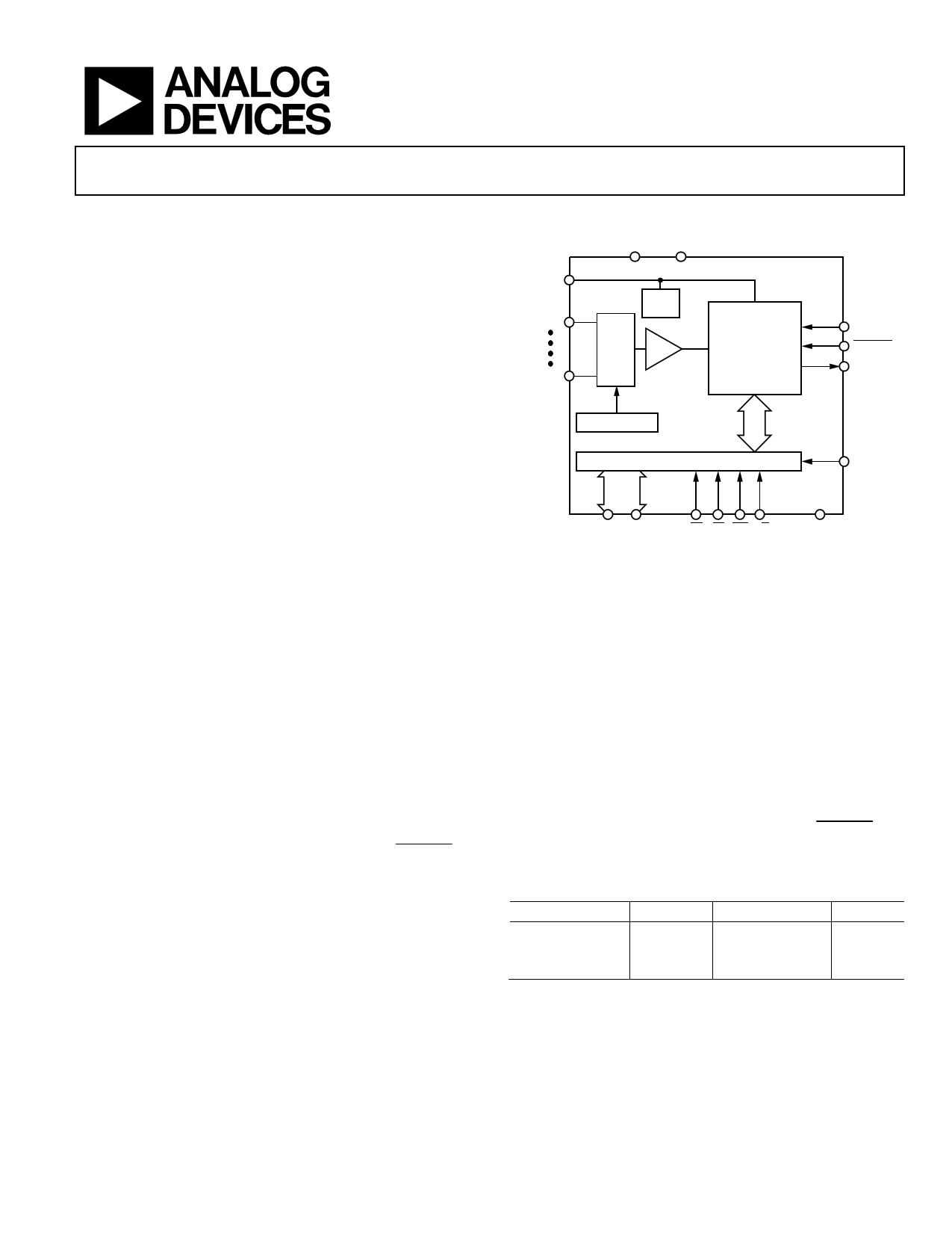
4-Channel, 625 kSPS, 12-Bit
Parallel ADC with a Sequencer
AD7934-6
VREFIN/
VREFOUT
VIN0
VIN3
FUNCTIONAL BLOCK DIAGRAM
VDD AGND
AD7934-6
2.5V
VREF
I/P
MUX
T/H
12-BIT
SAR ADC
AND
CONTROL
CLKIN
CONVST
BUSY
SEQUENCER
PARALLEL INTERFACE/CONTROL REGISTER
VDRIVE
DB0 DB11
CS RD WR W/B
Figure. 1
DGND
features flexible power management options. An on-chip control
register allows the user to set up different operating conditions,
including analog input range and configuration, output coding,
power management, and channel sequencing.
PRODUCT HIGHLIGHTS
1. High throughput with low power consumption.
2. Four analog inputs with a channel sequencer.
3. Accurate on-chip 2.5 V reference.
4. Single-ended, pseudo differential, or fully differential
analog inputs that are software selectable.
5. No pipeline delay.
6. Accurate control of the sampling instant via a CONVST
input and once-off conversion control.
Table 1. Related Devices
Similar Device No. of Bits
AD7938/AD7939 12/10
AD7933/AD7934 10/12
AD7938-6
12
No. of Channels
8
4
8
Speed
1.5 MSPS
1.5 MSPS
625 kSPS
Rev. B
Information furnished by Analog Devices is believed to be accurate and reliable. However, no
responsibility is assumed by Analog Devices for its use, nor for any infringements of patents or other
rights of third parties that may result from its use. Specifications subject to change without notice. No
license is granted by implication or otherwise under any patent or patent rights of Analog Devices.
Trademarksandregisteredtrademarksarethepropertyoftheirrespectiveowners.
One Technology Way, P.O. Box 9106, Norwood, MA 02062-9106, U.S.A.
Tel: 781.329.4700
www.analog.com
Fax: 781.461.3113 ©2005–2007 Analog Devices, Inc. All rights reserved.
1 page 
AD7934-6
Parameter
REFERENCE INPUT/OUTPUT
VREF Input Voltage5
DC Leakage Current4
VREFOUT Output Voltage
VREFOUT Temperature Coefficient
VREF Noise
VREF Output Impedance
VREF Input Capacitance
LOGIC INPUTS
Input High Voltage, VINH
Input Low Voltage, VINL
Input Current, IIN
Input Capacitance, CIN4
LOGIC OUTPUTS
Output High Voltage, VOH
Output Low Voltage, VOL
Floating-State Leakage Current
Floating-State Output Capacitance4
Output Coding
CONVERSION RATE
Conversion Time
Track-and-Hold Acquisition Time
Throughput Rate
POWER REQUIREMENTS
VDD
VDRIVE
IDD 6
Normal Mode (Static)
Normal Mode (Operational)
Autostandby Mode
Full/Autoshutdown Mode (Static)
Power Dissipation
Normal Mode (Operational)
Autostandby Mode (Static)
Full/Autoshutdown Mode
Value1
2.5
±1
2.5
25
5
10
130
10
15
25
2.4
0.8
±5
10
2.4
0.4
±3
10
Straight (natural) binary
Twos complement
t2 + 13 tCLKIN
125
80
625
2.7/5.25
2.7/5.25
0.8
1.5
1.2
0.3
160
2
7.5
3.6
800
480
10
6
Unit Test Conditions/Comments
V
μA max
V
ppm/°C max
ppm/°C typ
μV typ
μV typ
Ω typ
pF typ
pF typ
±1% for specified performance
±0.2% max @ 25°C
0.1 Hz to 10 Hz bandwidth
0.1 Hz to 1 MHz bandwidth
When in track
When in hold
V min
V max
μA max
pF max
Typically 10 nA, VIN = 0 V or VDRIVE
V min
V max
μA max
pF max
ISOURCE = 200 μA
ISINK = 200 μA
CODING bit = 0
CODING bit = 1
ns
ns max
ns typ
kSPS max
Full-scale step input
Sine wave input
V min/max
V min/max
mA typ
mA max
mA max
mA typ
μA typ
μA max
Digital I/PS = 0 V or VDRIVE
VDD = 2.7 V to 5.25 V, SCLK on or off
VDD = 4.75 V to 5.25 V
VDD = 2.7 V to 3.6 V
fSAMPLE = 100 kSPS, VDD = 5 V
Static, VDD = 3 V
SCLK on or off
mW max
mW max
μW typ
μW typ
μW max
μW max
VDD = 5 V
VDD = 3 V
VDD = 5 V
VDD = 3 V
VDD = 5 V
VDD = 3 V
1 Temperature range is as follows: B Version: −40°C to +85°C.
2 See the Terminology section.
3 VCM is the common-mode voltage. For full common-mode range, see Figure 25 and Figure 26. VIN+ and VIN− must always remain within GND/VDD.
4 Sample tested during initial release to ensure compliance.
5 This device is operational with an external reference in the range of 0.1 V to VDD. See the Reference section for more information.
6 Measured with a midscale dc analog input.
Rev. B | Page 4 of 28
5 Page 
AD7934-6
4
SINGLE-ENDED MODE
3
2
1 POSITIVE DNL
0
NEGATIVE DNL
–1
0.25 0.50 0.75 1.00 1.25 1.50 1.75 2.00 2.25 2.50 2.75
VREF (V)
Figure 9. DNL vs. VREF for VDD = 3 V
12
11
VDD = 5V
DIFFERENTIAL MODE
10 VDD = 5V
SINGLE-ENDED MODE
9
VDD = 3V
SINGLE-ENDED MODE
8 VDD = 3V
DIFFERENTIAL MODE
7
6
0 0.5 1.0 1.5 2.0 2.5 3.0 3.5 4.0
VREF (V)
Figure 10. ENOB vs. VREF
0
–0.5
–1.0
–1.5
–2.0
–2.5
–3.0
–3.5
–4.0
–4.5
–5.0
0
VDD = 5V
VDD = 3V
SINGLE-ENDED MODE
0.5 1.0 1.5 2.0 2.5 3.0 3.5
VREF (V)
Figure 11. Offset vs. VREF
10000
9000
DIFFERENTIAL MODE
9997
CODES
INTERNAL
REF
8000
7000
6000
5000
4000
3000
2000
1000
0
2046
2047
3 CODES
2048
2049
CODE
2050
Figure 12. Histogram of Codes for 10,000 Samples @ VDD = 5 V
with Internal Reference
120
DIFFERENTIAL MODE
110
100
90
80
70
60
0
200
400
600
800
1000
1200
RIPPLE FREQUENCY (kHz)
Figure 13. CMRR vs. Ripple Frequency with VDD = 5 V and 3 V
Rev. B | Page 10 of 28
11 Page | ||
| Páginas | Total 29 Páginas | |
| PDF Descargar | [ Datasheet AD7934-6.PDF ] | |
Hoja de datos destacado
| Número de pieza | Descripción | Fabricantes |
| AD7934-6 | 12-Bit Parallel ADC | Analog Devices |
| Número de pieza | Descripción | Fabricantes |
| SLA6805M | High Voltage 3 phase Motor Driver IC. |
Sanken |
| SDC1742 | 12- and 14-Bit Hybrid Synchro / Resolver-to-Digital Converters. |
Analog Devices |
|
DataSheet.es es una pagina web que funciona como un repositorio de manuales o hoja de datos de muchos de los productos más populares, |
| DataSheet.es | 2020 | Privacy Policy | Contacto | Buscar |