|
|
|
PDF AD9577 Data sheet ( Hoja de datos )
| Número de pieza | AD9577 | |
| Descripción | Clock Generator | |
| Fabricantes | Analog Devices | |
| Logotipo | ||
Hay una vista previa y un enlace de descarga de AD9577 (archivo pdf) en la parte inferior de esta página. Total 30 Páginas | ||
|
No Preview Available !
Data Sheet
Clock Generator with Dual PLLs,
Spread Spectrum, and Margining
AD9577
FEATURES
Fully integrated dual PLL/VCO cores
1 integer-N and 1 fractional-N PLL
Continuous frequency coverage from 11.2 MHz to 200 MHz
Most frequencies from 200 MHz to 637.5 MHz available
PLL1 phase jitter (12 kHz to 20 MHz): 460 fs rms typical
PLL2 phase jitter (12 kHz to 20 MHz)
Integer-N mode: 470 fs rms typical
Fractional-N mode: 660 fs rms typical
Input crystal or reference clock frequency
Optional reference frequency divide-by-2
I2C programmable output frequencies
Up to 4 LVDS/LVPECL or up to 8 LVCMOS output clocks
1 CMOS buffered reference clock output
Spread spectrum: downspread [0, −0.5]%
2 pin-controlled frequency maps: margining
Integrated loop filters
Space saving, 6 mm × 6 mm, 40-lead LFCSP package
1.02 W power dissipation (LVDS operation)
1.235 W power dissipation (LVPECL operation)
3.3 V operation
APPLICATIONS
Low jitter, low phase noise multioutput clock generator for
data communications applications including Ethernet,
Fibre Channel, SONET, SDH, PCI-e, SATA, PTN, OTN,
ADC/DAC, and digital video
Spread spectrum clocking
GENERAL DESCRIPTION
The AD9577 provides a multioutput clock generator function,
along with two on-chip phase-locked loop cores, PLL1 and PLL2,
optimized for network clocking applications. The PLL designs
are based on the Analog Devices, Inc., proven portfolio of high
performance, low jitter frequency synthesizers to maximize
network performance. The PLLs have I2C programmable output
frequencies and formats. The fractional-N PLL can support
spread spectrum clocking for reduced EMI radiated peak power.
Both PLLs can support frequency margining. Other applications
with demanding phase noise and jitter requirements can benefit
from this part.
The first integer-N PLL section (PLL1) consists of a low noise phase
frequency detector (PFD), a precision charge pump (CP), a low
phase noise voltage controlled oscillator (VCO), a programmable
Rev. A
Document Feedback
Information furnished by Analog Devices is believed to be accurate and reliable. However, no
responsibilityisassumedbyAnalogDevices for itsuse,nor foranyinfringementsofpatentsor other
rights of third parties that may result from its use. Specifications subject to change without notice. No
license is granted by implication or otherwise under any patent or patent rights of Analog Devices.
Trademarksandregisteredtrademarksarethepropertyoftheirrespectiveowners.
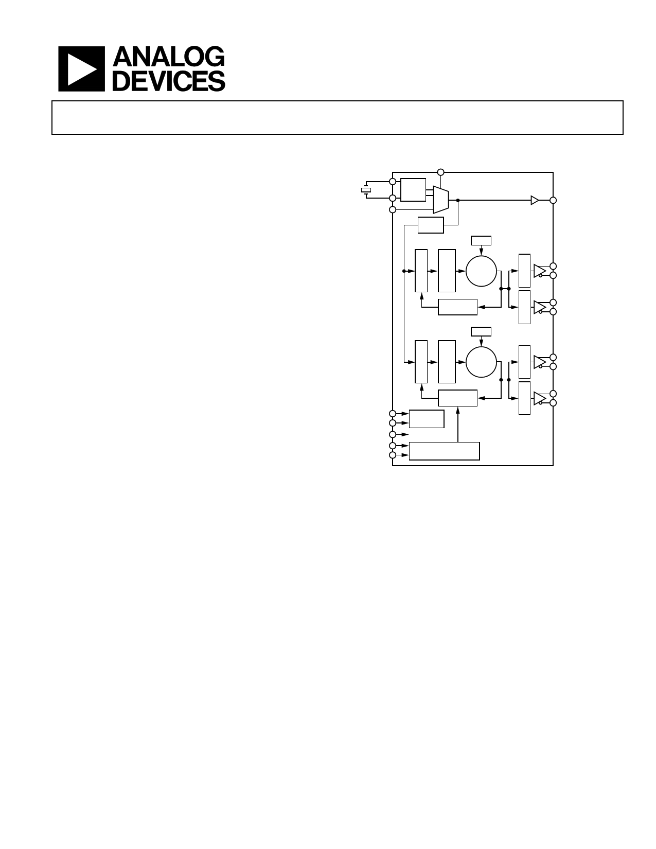
FUNCTIONAL BLOCK DIAGRAM
REFSEL
XT1
XT2
REFCLK
XTAL
OSC
DIVIDE
1 OR 2
PLL1
LDO
VCO
2.15GHz
TO
2.55GHz
CMOS
REFOUT
LVPECL/LVDS
OR 2 × CMOS
FEEDBACK
DIVIDER
PLL2
LDO
VCO
2.15GHz
TO
2.55GHz
LVPECL/LVDS
OR 2 × CMOS
LVPECL/LVDS
OR 2 × CMOS
SCL
SDA
MARGIN
SSCG
MAX_BW
FEEDBACK
DIVIDER
I2C
CONTROL
SPREAD SPECTRUM,
SDM
LVPECL/LVDS
OR 2 × CMOS
AD9577
Figure 1.
feedback divider, and two independently programmable output
dividers. By connecting an external crystal or applying a reference
clock to the REFCLK pin, frequencies of up to 637.5 MHz can
be synchronized to the input reference. Each output divider and
feedback divider ratio is I2C programmed for the required
output rates.
A second fractional-N PLL (PLL2) with a programmable modulus
allows VCO frequencies that are fractional multiples of the
reference frequency to be synthesized. Each output divider
and feedback divider ratio can be programmed for the required
output rates, up to 637.5 MHz. This fractional-N PLL can also
operate in integer-N mode for the lowest jitter.
Up to four differential output clock signals can be configured
as either LVPECL or LVDS signaling formats. Alternatively,
the outputs can be configured for up to eight CMOS outputs.
Combinations of these formats are supported. No external loop
filter components are required, thus conserving valuable design
time and board space. The AD9577 is available in a 40-lead, 6 mm ×
6 mm LFCSP package and can operate from a single 3.3 V supply.
The operating temperature range is −40°C to +85°C.
One Technology Way, P.O. Box 9106, Norwood, MA 02062-9106, U.S.A.
Tel: 781.329.4700 ©2011–2016 Analog Devices, Inc. All rights reserved.
Technical Support
www.analog.com
1 page 
AD9577
Parameter
Phase Noise (106.25 MHz CMOS Output)
At 1 kHz
At 10 kHz
At 100 kHz
At 1 MHz
At 10 MHz
At 30 MHz
Phase Noise (156.25 MHz CMOS Output)
At 1 kHz
At 10 kHz
At 100 kHz
At 1 MHz
At 10 MHz
At 30 MHz
Phase Noise (155.52 MHz LVPECL Output)
At 1 kHz
At 10 kHz
At 100 kHz
At 1 MHz
At 10 MHz
At 30 MHz
Phase Noise (622.08 MHz LVPECL Output)
At 1 kHz
At 10 kHz
At 100 kHz
At 1 MHz
At 10 MHz
At 30 MHz
Phase Noise (155.52 MHz LVDS Output)
At 1 kHz
At 10 kHz
At 100 kHz
At 1 MHz
At 10 MHz
At 30 MHz
Phase Noise (622.08 MHz LVDS Output)
At 1 kHz
At 10 kHz
At 100 kHz
At 1 MHz
At 10 MHz
At 30 MHz
Phase Noise (155.52 MHz CMOS Output)
At 1 kHz
At 10 kHz
At 100 kHz
At 1 MHz
At 10 MHz
At 30 MHz
1 x indicates either 0 or 1 for any given test condition.
Data Sheet
Min Typ
−118
−127
−127
−149
−156
−157
−115
−124
−124
−146
−155
−155
−117
−122
−123
−148
−156
−156
−105
−110
−110
−136
−150
−150
−117
−122
−123
−146
−155
−155
−105
−110
−110
−134
−149
−150
−117
−122
−123
−147
−155
−155
Max Unit
dBc/Hz
dBc/Hz
dBc/Hz
dBc/Hz
dBc/Hz
dBc/Hz
dBc/Hz
dBc/Hz
dBc/Hz
dBc/Hz
dBc/Hz
dBc/Hz
dBc/Hz
dBc/Hz
dBc/Hz
dBc/Hz
dBc/Hz
dBc/Hz
dBc/Hz
dBc/Hz
dBc/Hz
dBc/Hz
dBc/Hz
dBc/Hz
dBc/Hz
dBc/Hz
dBc/Hz
dBc/Hz
dBc/Hz
dBc/Hz
dBc/Hz
dBc/Hz
dBc/Hz
dBc/Hz
dBc/Hz
dBc/Hz
dBc/Hz
dBc/Hz
dBc/Hz
dBc/Hz
dBc/Hz
dBc/Hz
Test Conditions/Comments1
Na = 102, Vx = 4, Dx = 6, fPFD = 25 MHz
Na = 100, Vx = 4, Dx = 4, fPFD = 25 MHz
Na = 112, Vx = 2, Dx = 7, fPFD = 19.44 MHz
Na = 128, Vx = 2, Dx = 2, fPFD = 19.44 MHz
Na = 112, Vx = 2, Dx = 7, fPFD = 19.44 MHz
Na = 128, Vx = 2, Dx = 2, fPFD = 19.44 MHz
Na = 112, Vx = 2, Dx = 7, fPFD = 19.44 MHz
Rev. A | Page 4 of 44
5 Page 
AD9577
Data Sheet
Parameter1
CMOS INTEGRATED RANDOM PHASE JITTER
RMS Jitter (155.52 MHz Output)
RMS Jitter (38.88 MHz Output)
LVPECL PERIOD AND CYCLE-TO-CYCLE JITTER (100 MHz OUTPUT)
Output Peak-to-Peak Period Jitter
Output RMS Period Jitter
Output Peak-to-Peak, Cycle-to-Cycle Jitter
Output RMS Cycle-to-Cycle Jitter
LVDS PERIOD AND CYCLE-TO-CYCLE JITTER (100 MHz OUTPUT)
Output Peak-to-Peak Period Jitter
Output RMS Period Jitter
Output Peak-to-Peak, Cycle-to-Cycle Jitter
Output RMS Cycle-to-Cycle Jitter
CMOS PERIOD AND CYCLE-TO-CYCLE JITTER (100 MHz OUTPUT)
Output Peak-to-Peak Period Jitter
Output RMS Period Jitter
Output Peak-to-Peak, Cycle-to-Cycle
Output RMS Cycle-to-Cycle Jitter
LVPECL PERIOD AND CYCLE-TO-CYCLE JITTER (100 MHz OUTPUT)
Output Peak-to-Peak Period Jitter
Output RMS Period Jitter
Output Peak-to-Peak, Cycle-to-Cycle Jitter
Output RMS Cycle-to-Cycle Jitter
LVDS PERIOD AND CYCLE-TO-CYCLE JITTER (100 MHz OUTPUT)
Output Peak-to-Peak Period Jitter
Output RMS Period Jitter
Output Peak-to-Peak, Cycle-to-Cycle Jitter
Output RMS Cycle-to-Cycle Jitter
CMOS PERIOD AND CYCLE-TO-CYCLE JITTER (100 MHz OUTPUT)
Output Peak-to-Peak Period Jitter
Output RMS Period Jitter
Output Peak-to-Peak, Cycle-to-Cycle Jitter
Output RMS Cycle-Cycle Jitter
Min Typ Max Unit Test Conditions/Comments2
19.44 MHz crystal used, 50 Ω load
470 700 fs rms 12 kHz to 20 MHz, integer-N operation,
Nb = 112, Vx = 2, Dx = 7
430 650 fs rms 12 kHz to 5 MHz, integer-N operation,
Nb = 112, Vx = 2, Dx = 28
25 MHz crystal used, integer-N
operation, Nb = 96, Vx = 4, Dx = 6
13 ps p-p 10,000 cycles, average of 25 measurements
2 ps rms 10,000 cycles, average of 25 measurements
19 ps p-p 1,000 cycles, average of 25 measurements
3 ps rms 1,000 cycles, average of 25 measurements
25 MHz crystal used, integer-N
operation, Nb = 96, Vx = 4, Dx = 6
17 ps p-p 10,000 cycles, average of 25 measurements
2 ps rms 10,000 cycles, average of 25 measurements
26 ps p-p 1,000 cycles, average of 25 measurements
4 ps rms 1,000 cycles, average of 25 measurements
25 MHz crystal used, 50 Ω load, integer-N
operation, Nb = 96, Vx = 4, Dx = 6
25 ps p-p 10,000 cycles, average of 25 measurements
3 ps rms 10,000 cycles, average of 25 measurements
36 ps p-p 1,000 cycles, average of 25 measurements
6 ps rms 1,000 cycles, average of 25 measurements
25 MHz crystal used, SSCG on, Nb = 100,
FRAC = 0, MOD = 1000, Vx = 5, Dx = 5,
CkDiv = 7, NumSteps = 59, FracStep = −8,
fOUT = 100 MHz with −0.5% downspread
at 30.2 kHz
60 ps p-p 10,000 cycles, average of 25 measurements
15 ps rms 10,000 cycles, average of 25 measurements
20 ps p-p 1,000 cycles, average of 25 measurements
3 ps rms 1,000 cycles, average of 25 measurements
25 MHz crystal used, SSCG on, Nb = 100,
FRAC = 0, MOD = 1000, Vx = 5, Dx = 5,
CkDiv = 7, NumSteps = 59, FracStep = −8,
fOUT = 100 MHz with −0.5% downspread
at 30.2 kHz
63 ps p-p 10,000 cycles, average of 25 measurements
15 ps rms 10,000 cycles, average of 25 measurements
25 ps p-p 1,000 cycles, average of 25 measurements
4 ps rms 1,000 cycles, average of 25 measurements
25 MHz crystal used, SSCG on, 50 Ω load,
Nb = 100, FRAC = 0, MOD = 1000, Vx = 5,
Dx = 5, CkDiv = 7, NumSteps = 59,
FracStep = −8, fOUT = 100 MHz with
−0.5% downspread at 30.2 kHz
70 ps p-p 10,000 cycles, average of 25 measurements
15 ps rms 10,000 cycles, average of 25 measurements
36 ps p-p 1,000 cycles, average of 25 measurements
6 ps rms 1,000 cycles, average of 25 measurements
Rev. A | Page 10 of 44
11 Page | ||
| Páginas | Total 30 Páginas | |
| PDF Descargar | [ Datasheet AD9577.PDF ] | |
Hoja de datos destacado
| Número de pieza | Descripción | Fabricantes |
| AD9571 | Ethernet Clock Generator | Analog Devices |
| AD9572 | Fiber Channel/Ethernet Clock Generator IC | Analog Devices |
| AD9573 | PCI-Express Clock Generator IC | Analog Devices |
| AD9574 | Ethernet/Gigabit Ethernet Clock Generator | Analog Devices |
| Número de pieza | Descripción | Fabricantes |
| SLA6805M | High Voltage 3 phase Motor Driver IC. |
Sanken |
| SDC1742 | 12- and 14-Bit Hybrid Synchro / Resolver-to-Digital Converters. |
Analog Devices |
|
DataSheet.es es una pagina web que funciona como un repositorio de manuales o hoja de datos de muchos de los productos más populares, |
| DataSheet.es | 2020 | Privacy Policy | Contacto | Buscar |