|
|
|
PDF AD8628 Data sheet ( Hoja de datos )
| Número de pieza | AD8628 | |
| Descripción | Rail-to-Rail Input/Output Operational Amplifier | |
| Fabricantes | Analog Devices | |
| Logotipo | ||
Hay una vista previa y un enlace de descarga de AD8628 (archivo pdf) en la parte inferior de esta página. Total 24 Páginas | ||
|
No Preview Available !
Data Sheet
Zero-Drift, Single-Supply, Rail-to-Rail
Input/Output Operational Amplifier
AD8628/AD8629/AD8630
FEATURES
Lowest auto-zero amplifier noise
Low offset voltage: 1 µV
Input offset drift: 0.002 µV/°C
Rail-to-rail input and output swing
5 V single-supply operation
High gain, CMRR, and PSRR: 130 dB
Very low input bias current: 100 pA maximum
Low supply current: 1.0 mA
Overload recovery time: 50 µs
No external components required
Qualified for automotive applications
APPLICATIONS
Automotive sensors
Pressure and position sensors
Strain gage amplifiers
Medical instrumentation
Thermocouple amplifiers
Precision current sensing
Photodiode amplifiers
GENERAL DESCRIPTION
This amplifier has ultralow offset, drift, and bias current.
The AD8628/AD8629/AD8630 are wide bandwidth auto-zero
amplifiers featuring rail-to-rail input and output swing and low
noise. Operation is fully specified from 2.7 V to 5 V single supply
(±1.35 V to ±2.5 V dual supply).
The AD8628/AD8629/AD8630 provide benefits previously
found only in expensive auto-zeroing or chopper-stabilized
amplifiers. Using Analog Devices, Inc., topology, these zero-
drift amplifiers combine low cost with high accuracy and low
noise. No external capacitor is required. In addition, the AD8628/
AD8629/AD8630 greatly reduce the digital switching noise
found in most chopper-stabilized amplifiers.
With an offset voltage of only 1 µV, drift of less than 0.005 μV/°C,
and noise of only 0.5 µV p-p (0 Hz to 10 Hz), the AD8628/
AD8629/AD8630 are suited for applications where error
sources cannot be tolerated. Position and pressure sensors,
medical equipment, and strain gage amplifiers benefit greatly
from nearly zero drift over their operating temperature range.
Many systems can take advantage of the rail-to-rail input and
output swings provided by the AD8628/AD8629/AD8630 to
reduce input biasing complexity and maximize SNR.
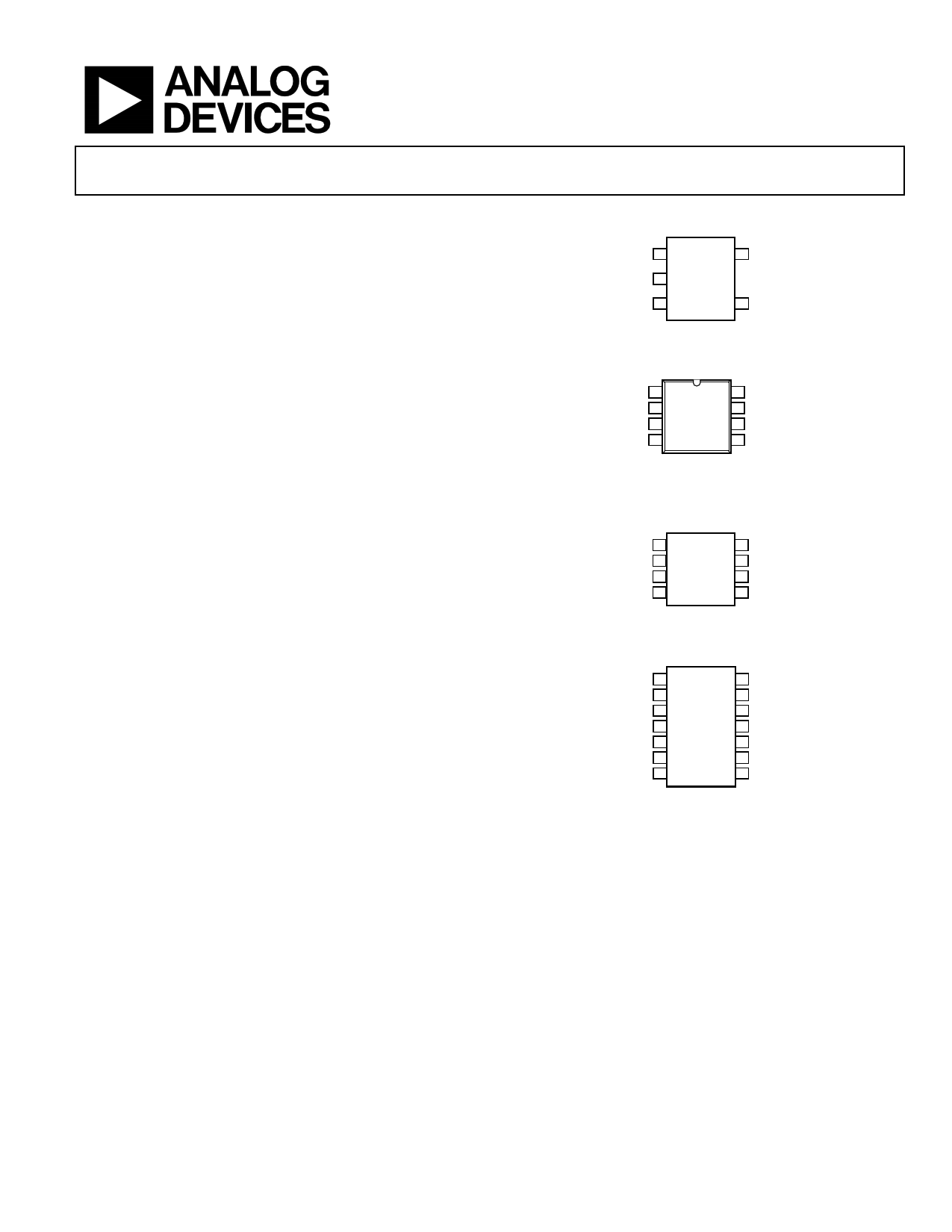
PIN CONFIGURATIONS
OUT 1
5 V+
AD8628
V– 2 TOP VIEW
(Not to Scale)
+IN 3
4 –IN
Figure 1. 5-Lead TSOT (UJ-5) and 5-Lead SOT-23 (RJ-5)
NC 1
8 NC
–IN 2 AD8628 7 V+
+IN 3 TOP VIEW 6 OUT
V– 4 (Not to Scale) 5 NC
NC = NO CONNECT
Figure 2. 8-Lead SOIC_N (R-8)
OUT A 1
8 V+
–IN A 2 AD8629 7 OUT B
+IN A
3
TOP VIEW
(Not to Scale)
6
–IN B
V– 4
5 +IN B
Figure 3. 8-Lead SOIC_N (R-8) and 8-Lead MSOP (RM-8)
OUT A 1
14 OUT D
–IN A 2
13 –IN D
+IN A 3 AD8630 12 +IN D
V+ 4 TOP VIEW 11 V–
+IN B 5 (Not to Scale) 10 +IN C
–IN B 6
9 –IN C
OUT B 7
8 OUT C
Figure 4. 14-Lead SOIC_N (R-14) and 14-Lead TSSOP (RU-14)
The AD8628/AD8629/AD8630 are specified for the extended
industrial temperature range (−40°C to +125°C). The AD8628
is available in tiny 5-lead TSOT, 5-lead SOT-23, and 8-lead
narrow SOIC plastic packages. The AD8629 is available in the
standard 8-lead narrow SOIC and MSOP plastic packages. The
AD8630 quad amplifier is available in 14-lead narrow SOIC and
14-lead TSSOP plastic packages. See the Ordering Guide for
automotive grades.
Rev. K
Document Feedback
Information furnished by Analog Devices is believed to be accurate and reliable. However, no
responsibilityisassumedbyAnalogDevices for itsuse,nor foranyinfringementsofpatentsor other
rights of third parties that may result from its use. Specifications subject to change without notice. No
license is granted by implication or otherwise under any patent or patent rights of Analog Devices.
Trademarksandregisteredtrademarksarethepropertyoftheirrespectiveowners.
One Technology Way, P.O. Box 9106, Norwood, MA 02062-9106, U.S.A.
Tel: 781.329.4700 ©2002–2014 Analog Devices, Inc. All rights reserved.
Technical Support
www.analog.com
1 page 
Data Sheet
AD8628/AD8629/AD8630
ELECTRICAL CHARACTERISTICS—VS = 2.7 V
VS = 2.7 V, VCM = 1.35 V, VO = 1.4 V, TA = 25°C, unless otherwise noted.
Table 2.
Parameter
INPUT CHARACTERISTICS
Offset Voltage
Input Bias Current
AD8628/AD8629
AD8630
Input Offset Current
Input Voltage Range
Common-Mode Rejection Ratio
Large Signal Voltage Gain
Offset Voltage Drift
OUTPUT CHARACTERISTICS
Output Voltage High
Output Voltage Low
Short-Circuit Limit
Output Current
POWER SUPPLY
Power Supply Rejection Ratio
Supply Current per Amplifier
INPUT CAPACITANCE
Differential
Common Mode
DYNAMIC PERFORMANCE
Slew Rate
Overload Recovery Time
Gain Bandwidth Product
NOISE PERFORMANCE
Voltage Noise
Voltage Noise Density
Current Noise Density
Symbol Conditions
VOS
−40°C ≤ TA ≤ +125°C
IB
IOS
CMRR
AVO
∆VOS/∆T
VOH
VOL
ISC
IO
PSRR
ISY
CIN
−40°C ≤ TA ≤ +125°C
−40°C ≤ TA ≤ +125°C
VCM = 0 V to 2.7 V
−40°C ≤ TA ≤ +125°C
RL = 10 kΩ, VO = 0.3 V to 2.4 V
−40°C ≤ TA ≤ +125°C
−40°C ≤ TA ≤ +125°C
RL = 100 kΩ to ground
−40°C ≤ TA ≤ +125°C
RL = 10 kΩ to ground
−40°C ≤ TA ≤ +125°C
RL = 100 kΩ to V+
−40°C ≤ TA ≤ +125°C
RL = 10 kΩ to V+
−40°C ≤ TA ≤ +125°C
−40°C ≤ TA ≤ +125°C
−40°C ≤ TA ≤ +125°C
VS = 2.7 V to 5.5 V, −40°C ≤ TA ≤ +125°C
VO = VS/2
−40°C ≤ TA ≤ +125°C
SR
GBP
en p-p
en
in
RL = 10 kΩ
0.1 Hz to 10 Hz
f = 1 kHz
f = 10 Hz
Min Typ Max Unit
1 5 µV
10 µV
30 100 pA
100 300 pA
1.0 1.5 nA
50 200 pA
250 pA
0 2.7 V
115 130
dB
110 120
dB
110 140
dB
105 130
dB
0.002 0.02 µV/°C
2.68 2.695
2.68 2.695
2.67 2.68
2.67 2.675
15
25
10 20
15 20
±10 ±15
±10
±10
±5
V
V
V
V
mV
mV
mV
mV
mA
mA
mA
mA
115 130
dB
0.75 1.0 mA
0.9 1.2 mA
1.5 pF
8.0 pF
1 V/µs
0.05 ms
2 MHz
0.5 µV p-p
22 nV/√Hz
5 fA/√Hz
Rev. K | Page 5 of 24
5 Page 
Data Sheet
VS = ±2.5V
VIN = 1kHz @ ±3V p-p
CL = 0pF
RL = 10kΩ
AV = 1
0V
TIME (200µs/DIV)
Figure 29. No Phase Reversal
140
VS = 2.7V
120
100
80
60
40
20
0
–20
–40
–60
100
1k 10k 100k
FREQUENCY (Hz)
Figure 30. CMRR vs. Frequency
1M
10M
140
VS = 5V
120
100
80
60
40
20
0
–20
–40
–60
100
1k 10k 100k
FREQUENCY (Hz)
Figure 31. CMRR vs. Frequency
1M
10M
AD8628/AD8629/AD8630
140
VS = ±1.35V
120
100
80
60
+PSRR
40
20 –PSRR
0
–20
–40
–60
100
1k 10k 100k
FREQUENCY (Hz)
Figure 32. PSRR vs. Frequency
1M
10M
140
VS = ±2.5V
120
100
80
60
+PSRR
40
–PSRR
20
0
–20
–40
–60
100
1k 10k 100k
FREQUENCY (Hz)
Figure 33. PSRR vs. Frequency
1M
10M
3.0
VS = 2.7V
RL = 10kΩ
2.5
TA = 25°C
AV = 1
2.0
1.5
1.0
0.5
0
100 1k 10k 100k
FREQUENCY (Hz)
Figure 34. Maximum Output Swing vs. Frequency
1M
Rev. K | Page 11 of 24
11 Page | ||
| Páginas | Total 24 Páginas | |
| PDF Descargar | [ Datasheet AD8628.PDF ] | |
Hoja de datos destacado
| Número de pieza | Descripción | Fabricantes |
| AD8620 | (AD8610 / AD8620) Wide Bandwidth JFET Operational Amplifier | Analog Devices |
| AD8622 | (AD8622 / AD8624) Precision Rail-to-Rail Output Op Amp | Analog Devices |
| AD8624 | (AD8622 / AD8624) Precision Rail-to-Rail Output Op Amp | Analog Devices |
| AD8625 | Precision Low Power Single-Supply JFET Amplifiers | Analog Devices |
| Número de pieza | Descripción | Fabricantes |
| SLA6805M | High Voltage 3 phase Motor Driver IC. |
Sanken |
| SDC1742 | 12- and 14-Bit Hybrid Synchro / Resolver-to-Digital Converters. |
Analog Devices |
|
DataSheet.es es una pagina web que funciona como un repositorio de manuales o hoja de datos de muchos de los productos más populares, |
| DataSheet.es | 2020 | Privacy Policy | Contacto | Buscar |