|
|
|
PDF AD8367 Data sheet ( Hoja de datos )
| Número de pieza | AD8367 | |
| Descripción | Linear-in-dB VGA | |
| Fabricantes | Analog Devices | |
| Logotipo | ||
Hay una vista previa y un enlace de descarga de AD8367 (archivo pdf) en la parte inferior de esta página. Total 25 Páginas | ||
|
No Preview Available !
FEATURES
Broad-range analog variable gain: −2.5 dB to +42.5 dB
3 dB cutoff frequency of 500 MHz
Gain up and gain down modes
Linear-in-dB, scaled 20 mV/dB
Resistive ground referenced input
Nominal ZIN = 200 Ω
On-chip, square-law detector
Single-supply operation: 2.7 V to 5.5 V
APPLICATIONS
Cellular base stations
Broadband access
Power amplifier control loops
Complete, linear IF AGC amplifiers
High speed data I/O
GENERAL DESCRIPTION
The AD8367 is a high performance 45 dB variable gain
amplifier with linear-in-dB gain control for use from low
frequencies up to several hundred megahertz. The range,
flatness, and accuracy of the gain response are achieved using
Analog Devices’ X-AMP® architecture, the most recent in a
series of powerful proprietary concepts for variable gain
applications, which far surpasses what can be achieved using
competing techniques.
The input is applied to a 9-stage, 200 Ω resistive ladder network.
Each stage has 5 dB of loss, giving a total attenuation of 45 dB.
At maximum gain, the first tap is selected; at progressively
lower gains, the tap moves smoothly and continuously toward
higher attenuation values. The attenuator is followed by a
42.5 dB fixed gain feedback amplifier—essentially an
operational amplifier with a gain bandwidth product of
100 GHz—and is very linear, even at high frequencies. The
output third order intercept is +20 dBV at 100 MHz (+27 dBm,
re 200 Ω), measured at an output level of 1 V p-p with VS = 5 V.
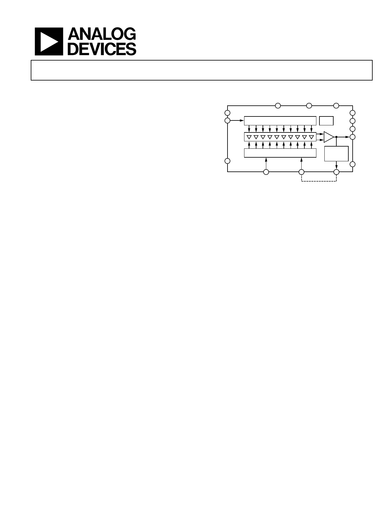
500 MHz, Linear-in-dB VGA
with AGC Detector
AD8367
ICOM 1
INPT 3
FUNCTIONAL BLOCK DIAGRAM
AD8367
VPSI
12
VPSO
11
ENBL
2
9-STAGE ATTENUATOR BY 5dB
BIAS
gm
CELLS
14 ICOM
9 DECL
13 HPFL
10 VOUT
ICOM 7
GAUSSIAN INTERPOLATOR
4
MODE
5
GAIN
Figure 1.
SQUARE
LAW
DETECTOR
8 OCOM
6
DETO
The analog gain-control input is scaled at 20 mV/dB and runs
from 50 mV to 950 mV. This corresponds to a gain of −2.5 dB
to +42.5 dB, respectively, when the gain up mode is selected and
+42.5 dB to −2.5 dB, respectively, when gain down mode is
selected. The gain down, or inverse, mode must be selected
when operating in AGC in which an integrated square-law
detector with an internal setpoint is used to level the output to
354 mV rms, regardless of the crest factor of the output signal.
A single external capacitor sets up the loop averaging time.
The AD8367 can be powered on or off by a voltage applied to
the ENBL pin. When this voltage is at a logic LO, the total
power dissipation drops to the milliwatt range. For a logic HI,
the chip powers up rapidly to its normal quiescent current of
26 mA at 25°C. The AD8367 is available in a 14-lead TSSOP
package for the industrial temperature range of −40°C to +85°C.
Rev. A
Information furnished by Analog Devices is believed to be accurate and reliable. However, no
responsibility is assumed by Analog Devices for its use, nor for any infringements of patents or other
rights of third parties that may result from its use. Specifications subject to change without notice. No
license is granted by implication or otherwise under any patent or patent rights of Analog Devices.
Trademarksandregisteredtrademarksarethepropertyoftheirrespectiveowners.
One Technology Way, P.O. Box 9106, Norwood, MA 02062-9106, U.S.A.
Tel: 781.329.4700
www.analog.com
Fax: 781.461.3113
© 2005 Analog Devices, Inc. All rights reserved.
1 page 
AD8367
Parameter
f = 140 MHz
Gain
Gain Scaling Factor
Gain Intercept
Noise Figure
Output IP3
Output 1 dB Compression Point
f = 190 MHz
Gain
Gain Scaling Factor
Gain Intercept
Noise Figure
Output IP3
Output 1 dB Compression Point
f = 240 MHz
Gain
Gain Scaling Factor
Gain Intercept
Noise Figure
Output IP3
Output 1 dB Compression Point
Conditions
Maximum gain
Minimum gain
Maximum gain
f1 = 140 MHz, f2 = 141 MHz, VGAIN = 0.5 V
VGAIN = 0.5 V
Maximum gain
Minimum gain
Maximum gain
f1 = 190 MHz, f2 = 191 MHz, VGAIN = 0.5 V
VGAIN = 0.5 V
Maximum gain
Minimum gain
Maximum gain
f1 = 240 MHz, f2 = 241 MHz, VGAIN = 0.5 V
VGAIN = 0.5 V
1 The output dc centering voltage is normally set at VS/2 and can be adjusted by applying a voltage to DECL.
Min Typ
Max Unit
+43.5
−3.6
19.7
−5.3
7.4
32.7
25.7
8.4
1.4
dB
dB
mV/dB
dB
dB
dBm
dBV rms
dBm
dBV rms
+43.5
−3.8
19.6
−5.3
7.5
30.9
23.9
8.4
1.4
dB
dB
mV/dB
dB
dB
dBm
dBV rms
dBm
dBV rms
+43 dB
−4.1 dB
19.7 mV/dB
−5.2 dB
7.6 dB
29.2 dBm
22.2 dBV rms
8.1 dBm
1.1 dBV rms
Rev. A | Page 4 of 24
5 Page 
AD8367
1.0 2.0
0.9
0.8
140MHz
70MHz
0.7
10MHz
70MHz
140MHz
240MHz
1.5
1.0
0.5
0.6 0
0.5 240MHz
0.4 10MHz
–0.5
–1.0
0.3 –1.5
0.2 –2.0
0.1 –2.5
0
–60 –50 –40 –30 –20 –10
INPUT LEVEL (dBV rms)
–3.0
0
Figure 21. AGC RSSI (Voltage on DETO Pin) vs. Input Power at 10 MHz,
70 MHz, 140 MHz, and 240 MHz
1.0
0.9
0.8
0.7
0.6
0.5
0.4
0.3
0.2
0.1
0
–60
+85°C +25°C
2.0
+25°C
–40°C
+85°C
1.5
1.0
0.5
0
–40°C
–0.5
–1.0
–1.5
–2.0
–2.5
–50 –40 –30 –20 –10
INPUT LEVEL (dBV rms)
Figure 22. AGC RSSI (Voltage on DETO Pin) vs.
Input Power over Temperature at 70 MHz
–3.0
0
1.0 2.5
0.9 2.0
0.8 1.5
0.7
WCDMA
1.0
256QAM 64QAM 16QAM
0.6 SINE 0.5
0.5 0
0.4 –0.5
IS95FWD
0.3 –1.0
0.2 –1.5
0.1 –2.0
0
–60 –50 –40 –30 –20 –10
INPUT LEVEL (dBV rms)
–2.5
0
Figure 23. AGC RSSI (Voltage on DETO Pin) vs. Input Power
for Various Modulation Schemes
0.8
VAGC
0.7
CAGC = 100pF
0.6
VOUT
0.5
0.4
–2–5
–1–5
0
TIME (Seconds)
1–5
Figure 24. AGC Time Domain Response (3 dB Step)
2–5
19.0097
19.7297
19.9097
20.0897
GAIN SCALING (mV/dB)
Figure 25. Gain Scaling Distribution at 70 MHz
20.2697
–6.4
–6.2
–6.0
–5.8 –5.6 –5.4
INTERCEPT (dB)
–5.2
–5.0
Figure 26. Gain Intercept Distribution at 70 MHz
–4.8
Rev. A | Page 10 of 24
11 Page | ||
| Páginas | Total 25 Páginas | |
| PDF Descargar | [ Datasheet AD8367.PDF ] | |
Hoja de datos destacado
| Número de pieza | Descripción | Fabricantes |
| AD8361 | LF to 2.5 GHz TruPwr Detector | Analog Devices |
| AD8362 | 50 Hz to 3.8 GHz 65 dB TruPwr Detector | Analog Devices |
| AD8363 | 50 dB TruPwr Detector | Analog Devices |
| AD8364 | LF to 2.7 GHz Dual 60 dB TruPwr Detector | Analog Devices |
| Número de pieza | Descripción | Fabricantes |
| SLA6805M | High Voltage 3 phase Motor Driver IC. |
Sanken |
| SDC1742 | 12- and 14-Bit Hybrid Synchro / Resolver-to-Digital Converters. |
Analog Devices |
|
DataSheet.es es una pagina web que funciona como un repositorio de manuales o hoja de datos de muchos de los productos más populares, |
| DataSheet.es | 2020 | Privacy Policy | Contacto | Buscar |