|
|
|
PDF AD9786 Data sheet ( Hoja de datos )
| Número de pieza | AD9786 | |
| Descripción | 200 MSPS/500 MSPS TxDAC+ | |
| Fabricantes | Analog Devices | |
| Logotipo | ||
Hay una vista previa y un enlace de descarga de AD9786 (archivo pdf) en la parte inferior de esta página. Total 30 Páginas | ||
|
No Preview Available !
16-Bit, 200 MSPS/500 MSPS TxDAC+® with
2×/4×/8× Interpolation and Signal Processing
AD9786
FEATURES
PRODUCT HIGHLIGHTS
16-bit resolution, 200 MSPS input data rate
IMD 90 dBc @10 MHz
1. 16-bit, high speed, interpolating TxDAC+.
Noise spectral density (NSD): −164 dBm/Hz @ 10 MHz
2. 2×/4×/8× user-selectable interpolating filter. The filter
WCDMA ACLR = 80 dBc @ 40 MHz IF
eases data rate and output signal reconstruction filter
DNL = ±0.3 LSB
requirements.
INL = ±0.6 LSB
Selectable 2×/4×/8× interpolation filters
3. 200 MSPS input data rate.
Selectable fDAC/2, fDAC/4, fDAC/8 modulation modes
Single- or dual-channel signal processing
Selectable image rejection Hilbert transform
Flexible calibration engine
4. Ultra high speed, 500 MSPS DAC conversion rate.
5. Flexible clock with single-ended or differential input.
CMOS, 1 V p-p sine wave, and LVPECL capability.
Direct IF transmission features
Serial control interface
Versatile clock and data interface
3.3 V-compatible digital interface
On-chip 1.2 V reference
80-lead, thermally enhanced, TQFP_EP package
6. Complete CMOS DAC function. It operates from a 3.1 V
to 3.5 V single analog (AVDD) supply, 2.5 V digital supply,
and a 3.3 V digital (DRVDD) supply. The DAC full-scale
current can be reduced for lower power operation, and
a sleep mode is provided for low power idle periods.
7. On-chip voltage reference. The AD9786 includes a
APPLICATIONS
1.20 V temperature-compensated band gap voltage
Base stations: multicarrier WCDMA, GSM/EDGE, TD-SCDMA,
IS136, TETRA
Instrumentation
RF signal generators, arbitrary waveform generators
HDTV transmitters
Broadband wireless systems
reference.
8. Multichip synchronization. Multiple AD9786 DACs can
be synchronized to a single master AD9786 to ease timing
design requirements and optimize image reject transmit
performance.
Digital radio links
Satellite systems
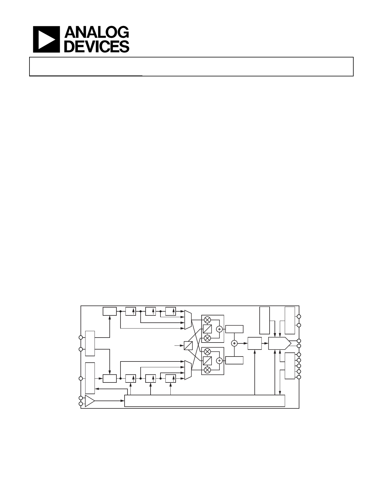
FUNCTIONAL BLOCK DIAGRAM
P1B[15:0]
P2B[15:0]
DATACLK
LATCH
2×
×1
LATCH
2×
2× 2×
I
fDAC/2
fDAC/4
fDAC/8
0
90
Q
2× 2×
0
90
0
90
Δt
ZERO
STUFF
16-BIT DAC
HILBERT
FSADJ
REFIO
IOUTA
IOUTB
SDIO
SDO
CSB
SCLK
RESET
CLK+
CLK–
CLOCK DISTRIBUTION AND CONTROL
Figure 1.
Rev. B
Information furnished by Analog Devices is believed to be accurate and reliable. However, no
responsibility is assumed by Analog Devices for its use, nor for any infringements of patents or other
rights of third parties that may result from its use. Specifications subject to change without notice. No
license is granted by implication or otherwise under any patent or patent rights of Analog Devices.
Trademarksandregisteredtrademarksarethepropertyoftheirrespectiveowners.
One Technology Way, P.O. Box 9106, Norwood, MA 02062-9106, U.S.A.
Tel: 781.329.4700
www.analog.com
Fax: 781.461.3113
© 2005 Analog Devices, Inc. All rights reserved.
1 page 
AD9786
GENERAL DESCRIPTION
The AD9786 is a 16-bit, high speed, CMOS DAC with
2×/4×/8× interpolation and signal processing features tuned
for communications applications. It offers state-of-the-art
distortion and noise performance. The AD9786 was developed
to meet the demanding performance requirements of multicarrier
and third-generation base stations. The selectable interpolation
filters simplify interfacing to a variety of input data rates while
also taking advantage of oversampling performance gains. The
modulation modes allow convenient bandwidth placement and
selectable sideband suppression.
The flexible clock interface accepts a variety of input types such
as 1 V p-p sine wave, CMOS, and LVPECL in single-ended or
differential mode. Internal dividers generate the required data
rate interface clocks.
The AD9786 provides a differential current output, supporting
single-ended or differential applications; it provides a nominal
full-scale current from 10 mA to 20 mA. The AD9786 is
manufactured on an advanced, low cost, 0.25 μm CMOS process.
Rev. B | Page 4 of 56
5 Page 
AD9786
ANALOG
Table 7. Analog Pin Function Descriptions
Pin No.
Mnemonic
59 REFIO
60 FSADJ
70, 71
IOUTB, IOUTA
61 DNC
62, 79
ADVDD
63, 78
ADGND
64, 77
ACVDD
65, 76
ACGND
66, 75
AVDD2
67, 74
AGND2
68, 73
AVDD1
69, 72
AGND1
80 DNC
Direction
A
A
A
Description
Reference.
Full-Scale Adjust.
Differential DAC Output Currents.
Do Not Connect.
Analog Domain Digital Content 2.5 V.
Analog Domain Digital Content 0 V.
Analog Domain Clock Content 2.5 V.
Analog Domain Clock Content 0 V.
Analog Domain Clock Switching 3.3 V.
Analog Domain Switching 0 V.
Analog Domain Quiet 3.3 V.
Analog Domain Quiet 0 V.
Do Not Connect.
DATA
Table 8. Data Pin Function Descriptions
Pin No.
Mnemonic
10 to 15, 18 to
24, 27 to 29
P1B15 to P1B0
32 IQSEL/P2B15
33 ONEPORTCLOCK/P2B14
34, 37 to 43,
46 to 51
30
9, 17, 26,
36, 44, 52
8, 16, 25,
35, 45, 53
P2B13 to P2B0
DRVDD
DVDD
DGND
Direction
I
I
I/O
I
Description
Input Data Port 1.
ONEPORT
0x02[6]
Mode
0 Latched data routed for I channel processing.
1 Latched data demultiplexed by IQSEL and routed for
interleaved I/Q processing.
ONEPORT
IQPOL IQSEL/
0x02[6]
0x02[1] P2B15 Mode (IQPOL = 0)
0 X X Latched data routed to Q channel Bit 15
(MSB) processing.
1 0 0 Latched data on Data Port 1 routed to Q
channel processing.
1 0 1 Latched data on Data Port 1 routed to I
channel processing.
1 1 0 Latched data on Data Port 1 routed to I
channel processing.
1 1 1 Latched data on Data Port 1 routed to Q
channel processing.
ONEPORT
0x02[6]
0 Latched data routed for Q channel Bit 14 processing.
1 Pin configured for output of clock at twice the channel
data route.
Input Data Port 2, Bit 13 to Bit 0.
Digital Output Pin Supply, 3.3 V.
Digital Domain, 2.5 V.
Digital Domain, 0 V.
Rev. B | Page 10 of 56
11 Page | ||
| Páginas | Total 30 Páginas | |
| PDF Descargar | [ Datasheet AD9786.PDF ] | |
Hoja de datos destacado
| Número de pieza | Descripción | Fabricantes |
| AD9780 | 500 MSPS DACs | Analog Devices |
| AD9781 | 500 MSPS DACs | Analog Devices |
| AD9782 | 200 MSPS/500 MSPS TxDAC | Analog Devices |
| AD9783 | 500 MSPS DACs | Analog Devices |
| Número de pieza | Descripción | Fabricantes |
| SLA6805M | High Voltage 3 phase Motor Driver IC. |
Sanken |
| SDC1742 | 12- and 14-Bit Hybrid Synchro / Resolver-to-Digital Converters. |
Analog Devices |
|
DataSheet.es es una pagina web que funciona como un repositorio de manuales o hoja de datos de muchos de los productos más populares, |
| DataSheet.es | 2020 | Privacy Policy | Contacto | Buscar |