|
|
|
PDF AD9741 Data sheet ( Hoja de datos )
| Número de pieza | AD9741 | |
| Descripción | 250 MSPS Digital-to-Analog Converters | |
| Fabricantes | Analog Devices | |
| Logotipo | ||
Hay una vista previa y un enlace de descarga de AD9741 (archivo pdf) en la parte inferior de esta página. Total 28 Páginas | ||
|
No Preview Available !
Data Sheet
Dual 8-/10-/12-/14-/16-Bit
250 MSPS Digital-to-Analog Converters
AD9741
FEATURES
High dynamic range, dual DACs
Low noise and intermodulation distortion
Single carrier WCDMA ACLR = 80 dBc at 61.44 MHz IF
Innovative switching output stage permits useable outputs
beyond Nyquist frequency
LVCMOS inputs with dual-port or optional interleaved
single-port operation
Differential analog current outputs are programmable from
8.6 mA to 31.7 mA full scale
Auxiliary 10-bit current DACs with source/sink capability for
external offset nulling
Internal 1.2 V precision reference voltage source
Operates from 1.8 V and 3.3 V supplies
315 mW power dissipation
Small footprint, Pb-free, 72-pin LFCSP
APPLICATIONS
Wireless infrastructure:
WCDMA, CDMA2000, TD-SCDMA, WiMAX
Wideband communications:
LMDS/MMDS, point-to-point
Instrumentation:
RF signal generators, arbitrary waveform generators
GENERAL DESCRIPTION
The AD9741/AD9743/AD9745/AD9746/AD9747 are pin-
compatible, high dynamic range, dual digital-to-analog
converters (DACs) with 8-/10-/12-/ 14-/16-bit resolutions
and sample rates of up to 250 MSPS. The devices include
specific features for direct conversion transmit applications,
including gain and offset compensation, and they interface
seamlessly with analog quadrature modulators, such as the
ADL5370.
A proprietary, dynamic output architecture permits synthesis
of analog outputs even above Nyquist by shifting energy away
from the fundamental and into the image frequency.
Full programmability is provided through a serial peripheral
interface (SPI) port. In addition, some pin-programmable
features are offered for those applications without a controller.
PRODUCT HIGHLIGHTS
1. Low noise and intermodulation distortion (IMD) enables
high quality synthesis of wideband signals.
2. Proprietary switching output for enhanced dynamic
performance.
3. Programmable current outputs and dual auxiliary DACs
provide flexibility and system enhancements.
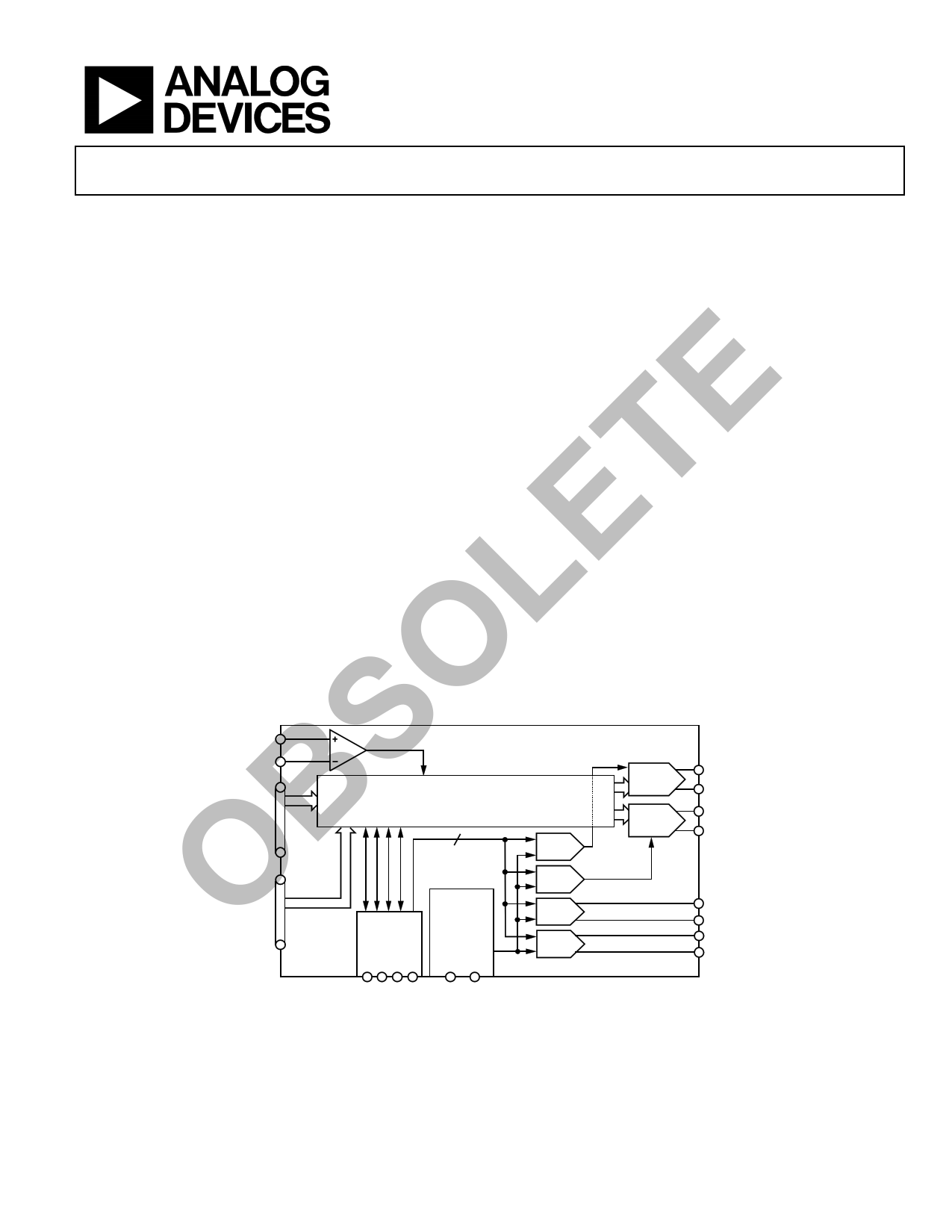
FUNCTIONAL BLOCK DIAGRAM
CLKP
CLKN
PID<15:0>
CMOS
INTERFACE
INTERFACE LOGIC
10
P2D<15:0>
SERIAL
PERIPHERAL
INTERFACE
INTERNAL
REFERENCE
AND
BIAS
GAIN
DAC
GAIN
DAC
OFFSET
DAC
OFFSET
DAC
16-BIT
DAC1
16-BIT
DAC2
IOUT1P
IOUT1N
IOUT2P
IOUT2N
AUX1P
AUX1N
AUX2P
AUX2N
Figure 1.
Rev. B
Document Feedback
Information furnished by Analog Devices is believed to be accurate and reliable. However, no
responsibilityisassumedbyAnalogDevices for itsuse,nor foranyinfringementsofpatentsor other
rights of third parties that may result from its use. Specifications subject to change without notice. No
license is granted by implication or otherwise under any patent or patent rights of Analog Devices.
Trademarksandregisteredtrademarksarethepropertyoftheirrespectiveowners.
One Technology Way, P.O. Box 9106, Norwood, MA 02062-9106, U.S.A.
Tel: 781.329.4700 ©2007–2014 Analog Devices, Inc. All rights reserved.
Technical Support
www.analog.com
1 page 
Data Sheet
AD9741
AC SPECIFICATIONS
TMIN to TMAX, AVDD33 = 3.3 V, DVDD33 = 3.3 V, DVDD18 = 1.8 V, CVDD18 = 1.8 V, IFS = 20 mA, full-scale digital input, maximum
sample rate, unless otherwise noted.
Table 3. AD9741, AD9743, and AD9745
Parameter
SPURIOUS FREE DYNAMIC RANGE (SFDR)
fDAC = 250 MSPS, fOUT = 20 MHz
fDAC = 250 MSPS, fOUT = 70 MHz
fDAC = 250 MSPS, fOUT = 180 MHz1
INTERMODULATION DISTORTION (IMD)
fDAC = 250 MSPS, fOUT = 20 MHz
fDAC = 250 MSPS, fOUT = 70 MHz
fDAC = 250 MSPS, fOUT = 180 MHz1
CROSSTALK
fDAC = 250 MSPS, fOUT = 20 MHz
fDAC = 250 MSPS, fOUT = 70 MHz
fDAC = 250 MSPS, fOUT = 180 MHz1
ADJACENT CHANNEL LEAKAGE RATIO (ACLR) SINGLE
CARRIER WCDMA
fDAC = 245.76 MSPS, fOUT = 15.36 MHz
fDAC = 245.76 MSPS, fOUT = 61.44 MHz
fDAC = 245.76 MSPS, fOUT = 184.32 MHz1
NOISE SPECTRAL DENSITY (NSD)
fDAC = 245.76 MSPS, fOUT = 15.36 MHz
fDAC = 245.76 MSPS, fOUT = 61.44 MHz
fDAC = 245.76 MSPS, fOUT = 184.32 MHz1
AD9741
AD9743
AD9745
Min Typ Max Min Typ Max Min Typ Max Unit
70 80 82 dBc
70 70 70 dBc
64 64 66 dBc
80 80 86 dBc
80 80 80 dBc
72 72 74 dBc
80 80 80 dBc
80 80 80 dBc
80 80 80 dBc
54
54
54
−132
−132
−135
66
66
64
−144
−144
−147
76
76
72
−155
−155
−155
dBc
dBc
dBc
dBm/Hz
dBm/Hz
dBm/Hz
1 Mix Mode.
Rev. B | Page 5 of 28
5 Page 
Data Sheet
AD9741
CVDD18 1
CVSS 2
CLKP 3
CLKN 4
CVSS 5
CVDD18 6
DVSS 7
DVDD18 8
P1D11 9
P1D10 10
P1D9 11
P1D8 12
P1D7 13
P1D6 14
P1D5 15
P1D4 16
P1D3 17
P1D2 18
NC = NO CONNECT
PIN 1
INDICATOR
AD9745
(TOP VIEW)
54 FSADJ
53 RESET
52 CSB
51 SCLK
50 SDIO
49 SDO
48 DVSS
47 DVDD18
46 NC
45 NC
44 NC
43 NC
42 P2D0
41 P2D1
40 P2D2
39 P2D3
38 P2D4
37 P2D5
Figure 4. AD9745 Pin Configuration
Table 10. AD9745 Pin Function Descriptions
Pin No.
Mnemonic Description
1, 6
CVDD18
Clock Supply Voltage (1.8 V).
2, 5
CVSS
Clock Supply Common (0 V).
3
CLKP
Differential DAC Clock Input.
4
CLKN
Complementary Differential DAC Clock Input.
7, 28, 48
DVSS
Digital Supply Common (0 V).
8, 47
DVDD18
Digital Core Supply Voltage (1.8 V).
9 to 20
P1D<11:0> Port 1 Data Bit Inputs.
21 to 24, 26, 30, 43 to 46 NC
No Connect.
25 DCO Data Clock Output. Use to clock data source.
27
DVDD33
Digital I/O Supply Voltage (3.3 V).
29
IQSEL
I/Q Framing Signal for Single-Port Mode Operation.
31 to 42
P2D<11:0> Port 2 Data Bit Inputs.
49 SDO Serial Peripheral Interface Data Output.
50
SDIO
Serial Peripheral Interface Data Input and Optional Data Output.
51
SCLK
Serial Peripheral Interface Clock Input.
52 CSB Serial Peripheral Interface Chip Select Input. Active low.
53
RESET
Hardware Reset. Active high.
54
FSADJ
Full-Scale Current Output Adjust. Connect 10 kΩ resistor to AVSS.
55
REFIO
Reference Input/Output. Connect a 0.1 μF capacitor to AVSS.
56, 57, 71, 72
AVDD33
Analog Supply Voltage (3.3 V).
58, 61, 64, 67, 70
AVSS
Analog Supply Common (0 V).
59
IOUT2P
DAC2 Current Output True. Sources full-scale current when input data bits are all 1.
60
IOUT2N
DAC2 Current Output Complement. Sources full-scale current when data bits are all 0.
62
AUX2P
Auxiliary DAC2 Default Current Output Pin.
63
AUX2N
Auxiliary DAC2 Optional Output Pin. Enable through SPI.
65
AUX1N
Auxiliary DAC1 Optional Output Pin. Enable through SPI.
66
AUX1P
Auxiliary DAC1 Default Current Output Pin.
68
IOUT1N
Complementary DAC1 Current Output. Sources full-scale current when data bits are all 0.
69
IOUT1P
DAC1 Current Output. Sources full-scale current when data bits are all 1.
EPAD
AVSS
Exposed Thermal Pad. Must be soldered to copper pour on top surface of PCB for mechanical
stability and must be electrically tied to low impedance GND plane for low noise performance.
Rev. B | Page 11 of 28
11 Page | ||
| Páginas | Total 28 Páginas | |
| PDF Descargar | [ Datasheet AD9741.PDF ] | |
Hoja de datos destacado
| Número de pieza | Descripción | Fabricantes |
| AD974 | 4-Channel/ 16-Bit/ 200 kSPS Data Acquisition System | Analog Devices |
| AD9740 | TxDAC D/A Converter | Analog Devices |
| AD9741 | 250 MSPS Digital-to-Analog Converters | Analog Devices |
| AD9742 | TxDAC Digital-to-Analog Converter | Analog Devices |
| Número de pieza | Descripción | Fabricantes |
| SLA6805M | High Voltage 3 phase Motor Driver IC. |
Sanken |
| SDC1742 | 12- and 14-Bit Hybrid Synchro / Resolver-to-Digital Converters. |
Analog Devices |
|
DataSheet.es es una pagina web que funciona como un repositorio de manuales o hoja de datos de muchos de los productos más populares, |
| DataSheet.es | 2020 | Privacy Policy | Contacto | Buscar |